

Circuit board and manufacturing method thereof
a technology of circuit boards and manufacturing methods, applied in the field of circuit boards, can solve the problems of reducing the yield in the manufacturing process of circuit boards, and achieve the effect of reducing the yield
- Summary
- Abstract
- Description
- Claims
- Application Information
AI Technical Summary
Benefits of technology
Problems solved by technology
Method used
Image

Examples
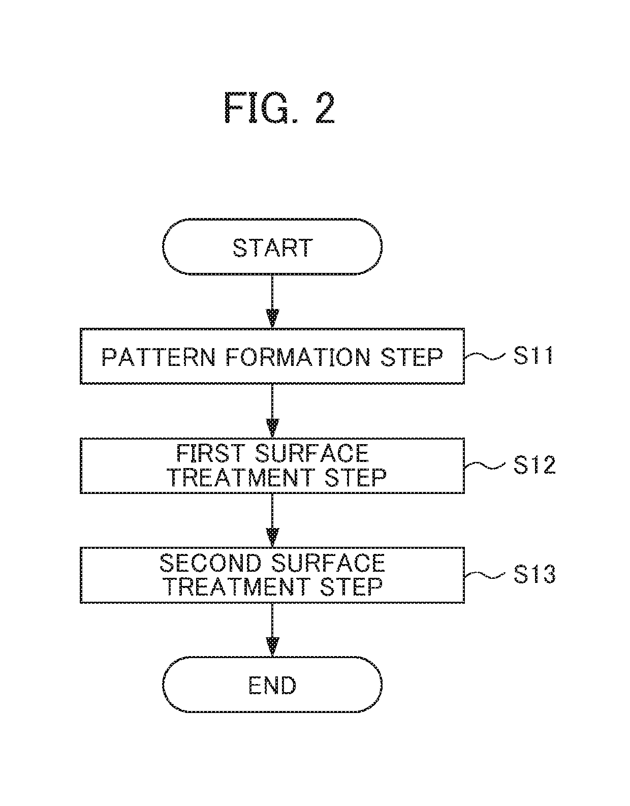
first embodiment
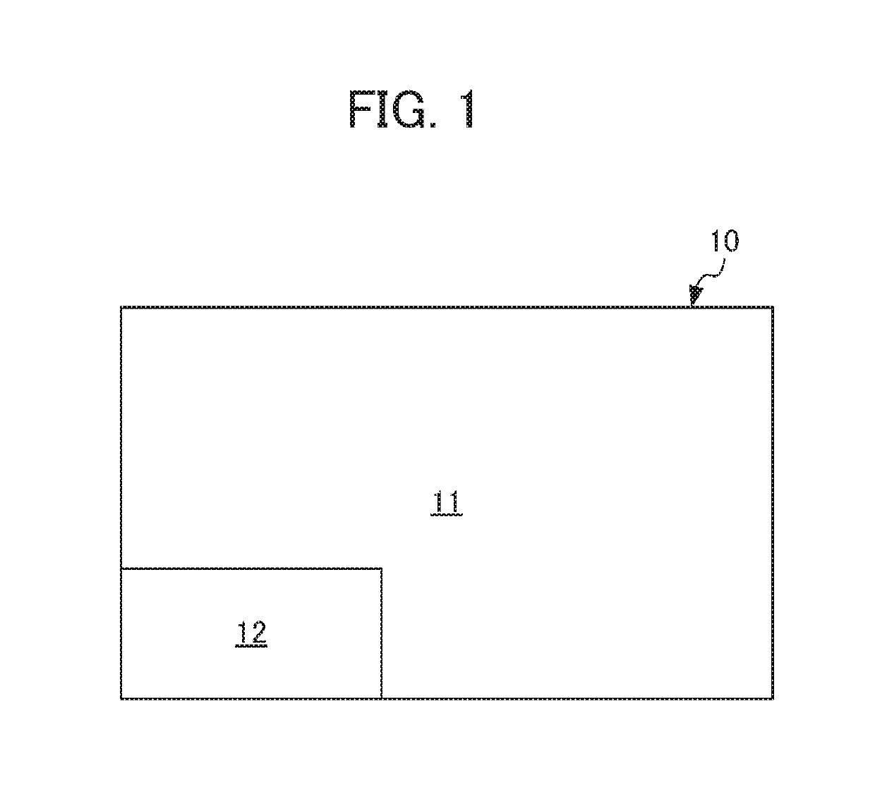
[0019]A circuit board 10 according to the first embodiment will first be described with reference to FIG. 1. FIG. 1 is a plan view of the circuit board 10.
[0020]As shown in FIG. 1, the circuit board 10 is obtained by providing a wiring pattern on an insulating board, and is applied to a machine tool, a robot controller and the like. The circuit board 10 includes a first region 11 and a second region 12.
[0021]In the first region 11, a first wiring pattern is provided on which a first surface treatment is applied. Examples of the first surface treatment include solder coat and Au flash.
[0022]In the second region 12, a second wiring pattern is provided on which a second surface treatment having a cutting fluid resistance lower than the first surface treatment is applied. The second region 12 includes a corner portion of the circuit board 10. Examples of the second surface treatment include pre-flux, Sn plating and Ag plating. Examples of the cutting fluid include a liquid containing ch...
second embodiment
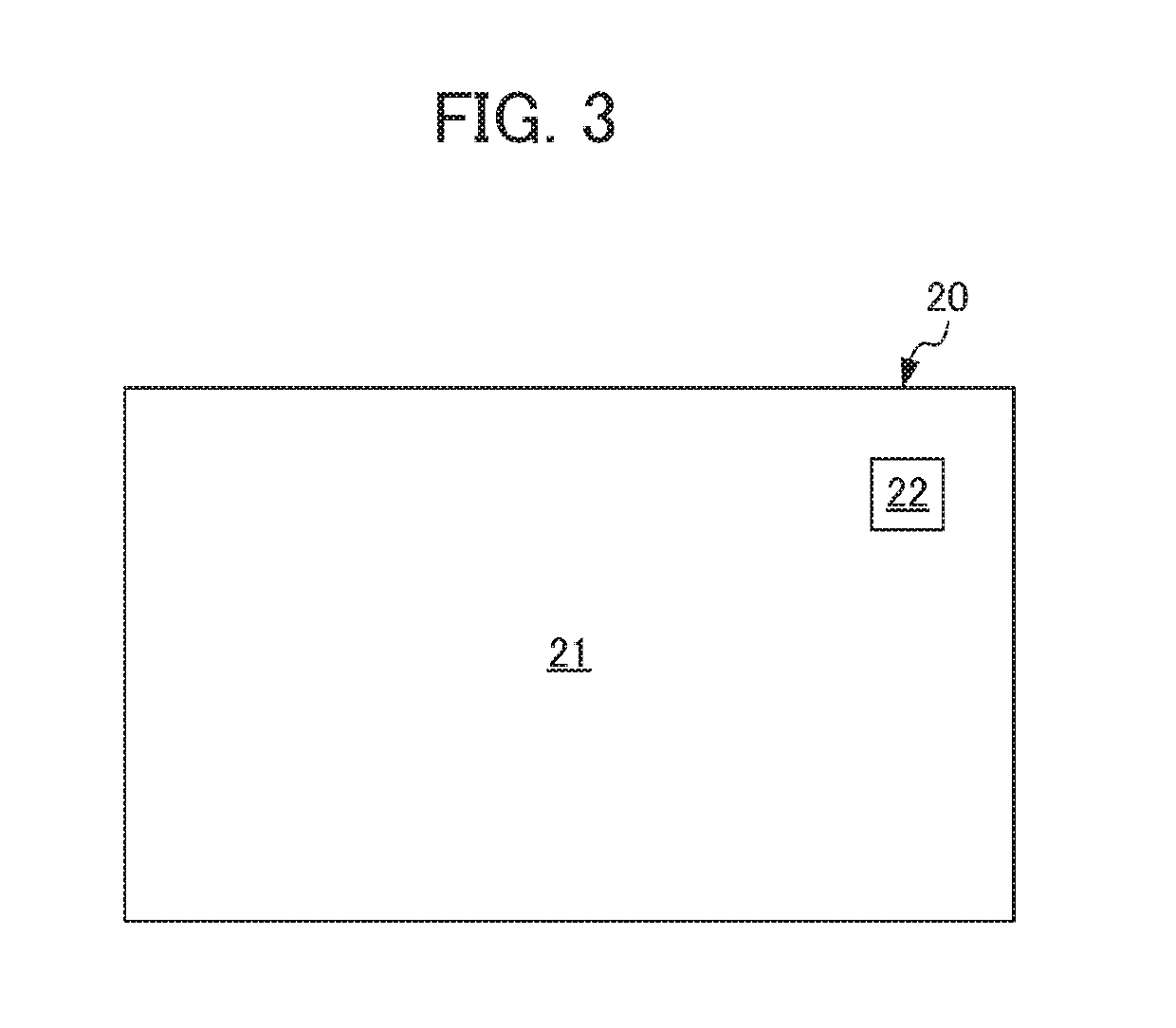
[0031]A circuit board 20 according to the second embodiment will then be described with reference to FIGS. 3 and 4. FIG. 3 is a plan view of the circuit board 20. FIG. 4 is a side cross-sectional view of the circuit board 20 shown in FIG. 3.
[0032]As shown in FIGS. 3 and 4, the circuit board 20 includes a first circuit board 21, a second circuit board 22, a pad 23 and a solder joint portion 24.
[0033]The first circuit board 21 is obtained by providing, on a first insulating board, a first wiring pattern on which a first surface treatment is applied. The first surface treatment in the second embodiment is the same as that in the first embodiment. On the first circuit board 21, the first surface treatment is totally applied. The outside shape of the first circuit board 21 agrees with the outside shape of the circuit board 20 in plan view.
[0034]The second circuit board 22 is obtained by providing, on a second insulating board, a second wiring pattern on which a second surface treatment i...
PUM
 Abstract
Description
Claims
Application Information