Electronic module and imaging system
- Summary
- Abstract
- Description
- Claims
- Application Information
AI Technical Summary
Benefits of technology
Problems solved by technology
Method used
Image
Examples
first embodiment
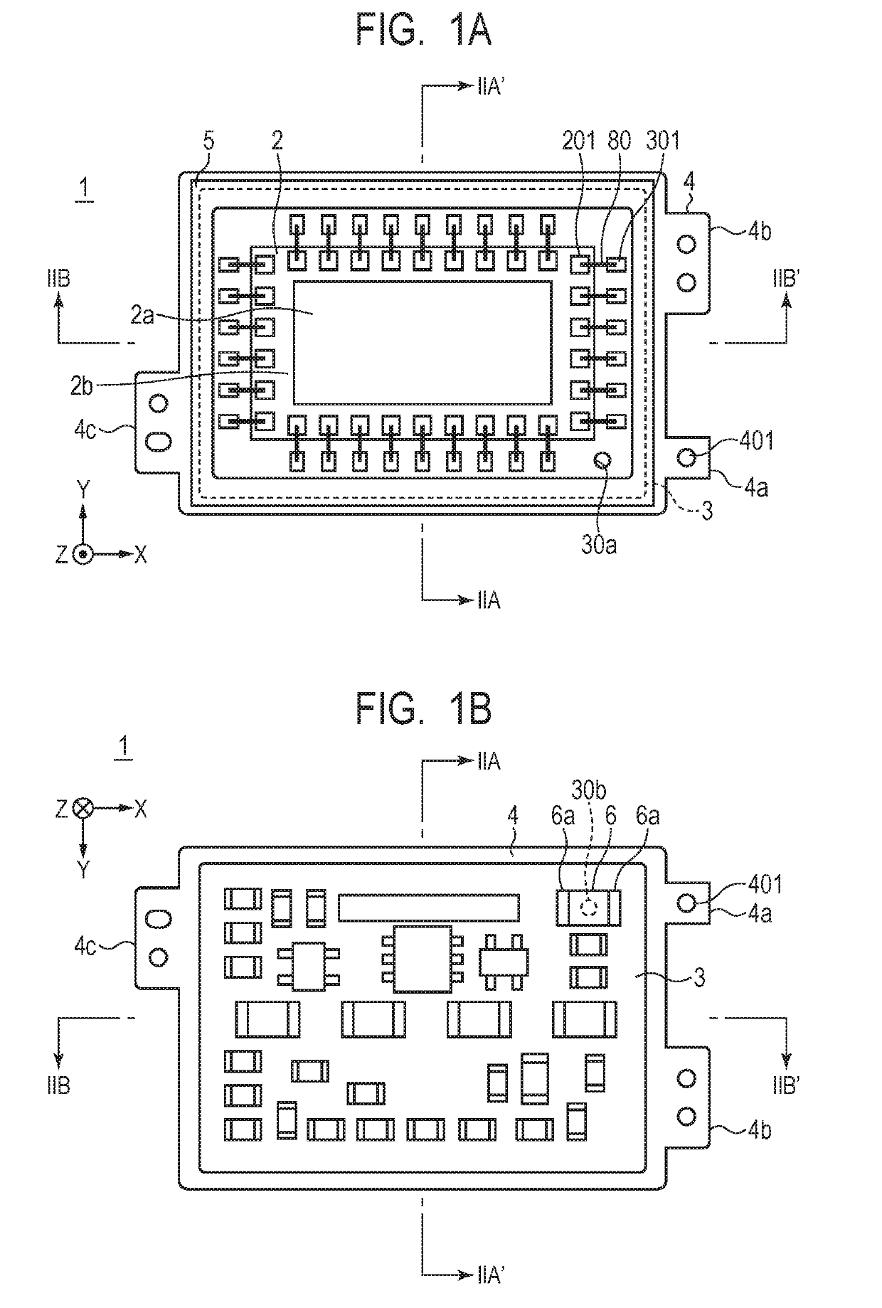
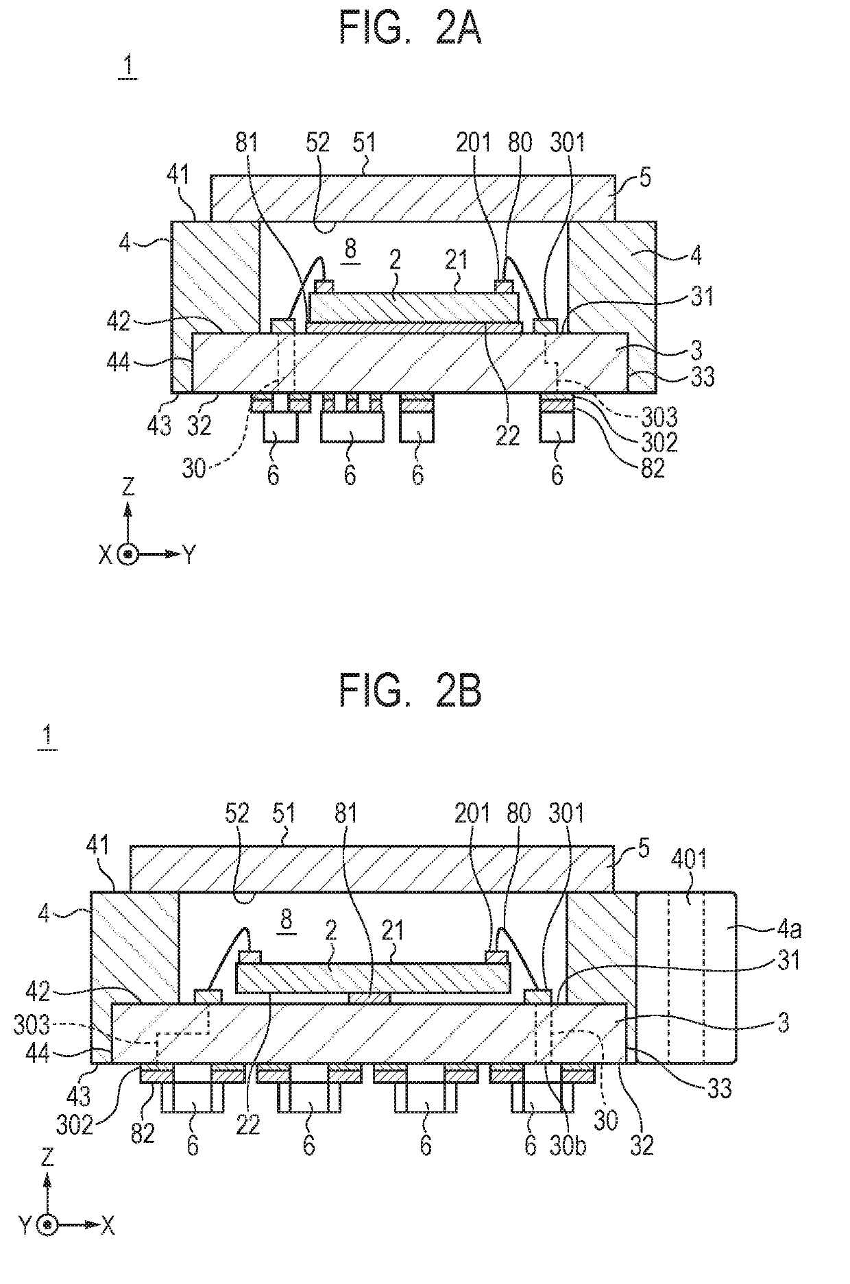
[0033]An electronic module according to a first embodiment of the present disclosure will be described below. FIG. 1A is a top view of an electronic module 1, and FIG. 1B is a bottom view of the electronic module 1. FIG. 2A is a sectional view of the electronic module 1 taken along a line IIA-IIA′ in FIG. 1A and FIG. 1B, and FIG. 2B is a sectional view of the electronic module 1 taken along a line IIB-IIB′. The same members are labelled with the common reference, and description will be provided below with reference to each diagram mutually.
[0034]In FIG. 1A, FIG. 1B, FIG. 2A, and FIG. 2B, the electronic module 1 has a planar shape with a predetermined height (thickness). The direction of the height of the electronic module 1 is here denoted as a Z-direction. Further, a longitudinal direction and a short direction of the electronic module 1 are denoted as an X-direction and a Y-direction, respectively. A typical electronic module 1 has a rectangular shape extending in the X-direction...
second embodiment
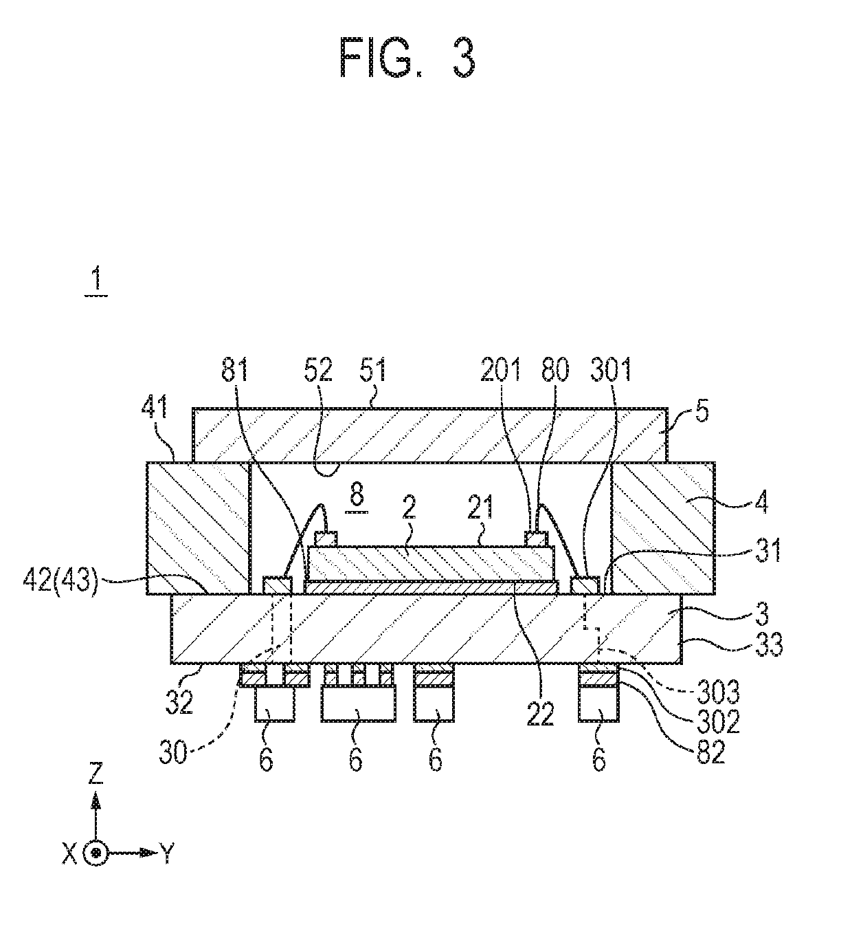
[0050]Next, an electronic module according to the present embodiment will be described mainly focusing on a configuration different from that of the first embodiment. FIG. 3 illustrates a sectional view of the electronic module 1 according to the present embodiment. The electronic module 1 illustrated in FIG. 3 is a modified example of the first embodiment, and a sectional view of a part corresponding to FIG. 2A is illustrated. In the present embodiment, the lower surface 42 of the frame 4 is formed flat, and the lowermost surface 43 of the frame 4 in the first embodiment corresponds to the lower surface 42 of the frame 4. The upper face 31 of the substrate 3 is adhered to the lower surface 42 of the frame 4. According to the present embodiment, a step between the lower surface 42 and the lowermost surface 43 of the frame 4 is not required to be formed, and thereby the frame 4 can be easily molded. Also in the present embodiment, the same advantage as that of the first embodiment ca...
third embodiment
[0051]FIG. 4 is a sectional view of an electronic module according to the present embodiment and illustrates a further modified example of the first embodiment. In the present embodiment, the recess 44 is formed on the inner periphery of the opening end of the frame 4, and the side end portion 33 of the substrate 3 is inserted into the recess 44. The upper face 31 of the substrate 3 comes into contact with the lower surface 42 of the frame 4, and the lowermost surface 43 of the frame 4 is located below the lower surface 32 of the substrate 3. In the present embodiment, the frame 4 is preferably formed so as to be in close contact with the substrate 3 by a resin molding method such as a transfer molding method.
[0052]Note that a surface of the frame 4 where the substrate 3 is fixed is not limited to that described in the first to third embodiments. Further, a method of fixing the substrate 3 to the frame 4 is not limited to a method using an adhesive material. When the frame 4 is made...
PUM
 Abstract
Description
Claims
Application Information


