

Circuit edit and obfuscation for trusted chip fabrication
a trusted chip and edit technology, applied in the direction of cad circuit design, instrumentation, semiconductor/solid-state device details, etc., can solve the problems of significant drawbacks in design overhead, cost, security, and increase the risk of security
Active Publication Date: 2019-10-10
UNIV OF FLORIDA RES FOUNDATION INC
View PDF0 Cites 13 Cited by
- Summary
- Abstract
- Description
- Claims
- Application Information
AI Technical Summary
Benefits of technology
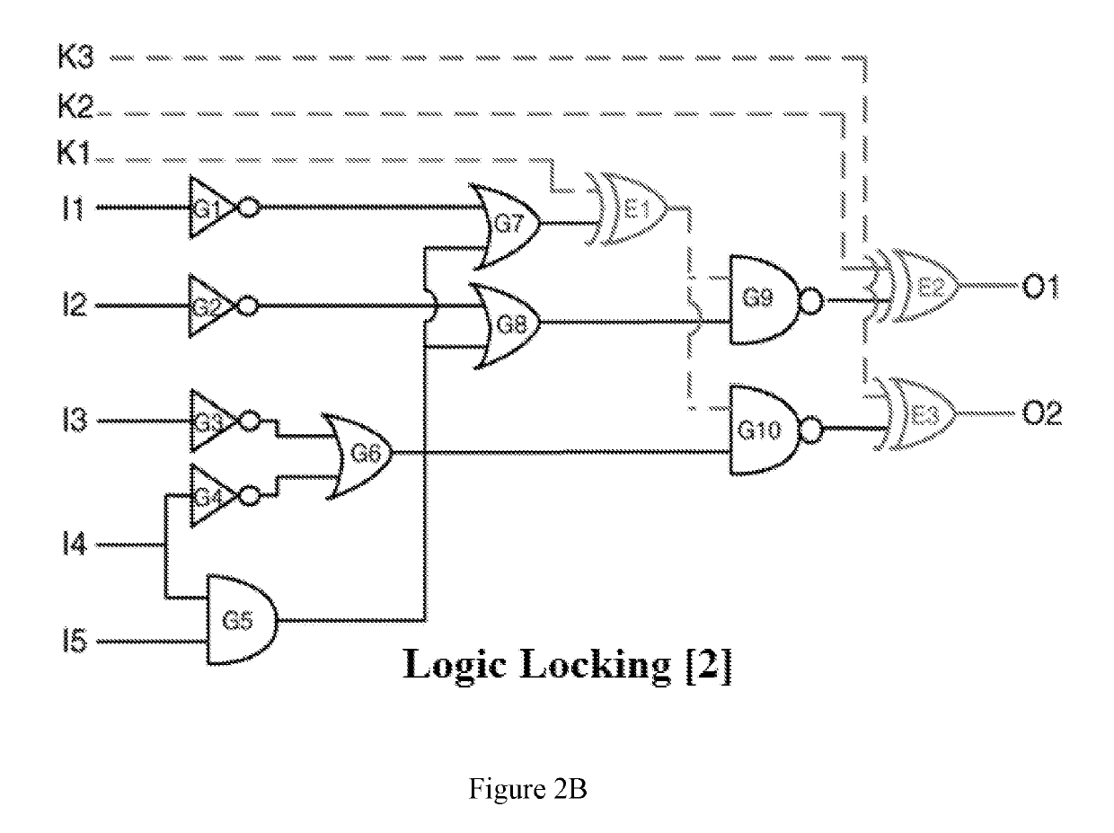
The patent text describes novel circuits and semiconductor devices that have one or more obfuscated circuits to protect IP or IC piracy. These circuits can change the output of an original circuit, and the output can be recovered by modifying the obfuscated circuit. The technical effect of this invention is to provide a secure method to prevent IP or IC piracy.
Problems solved by technology
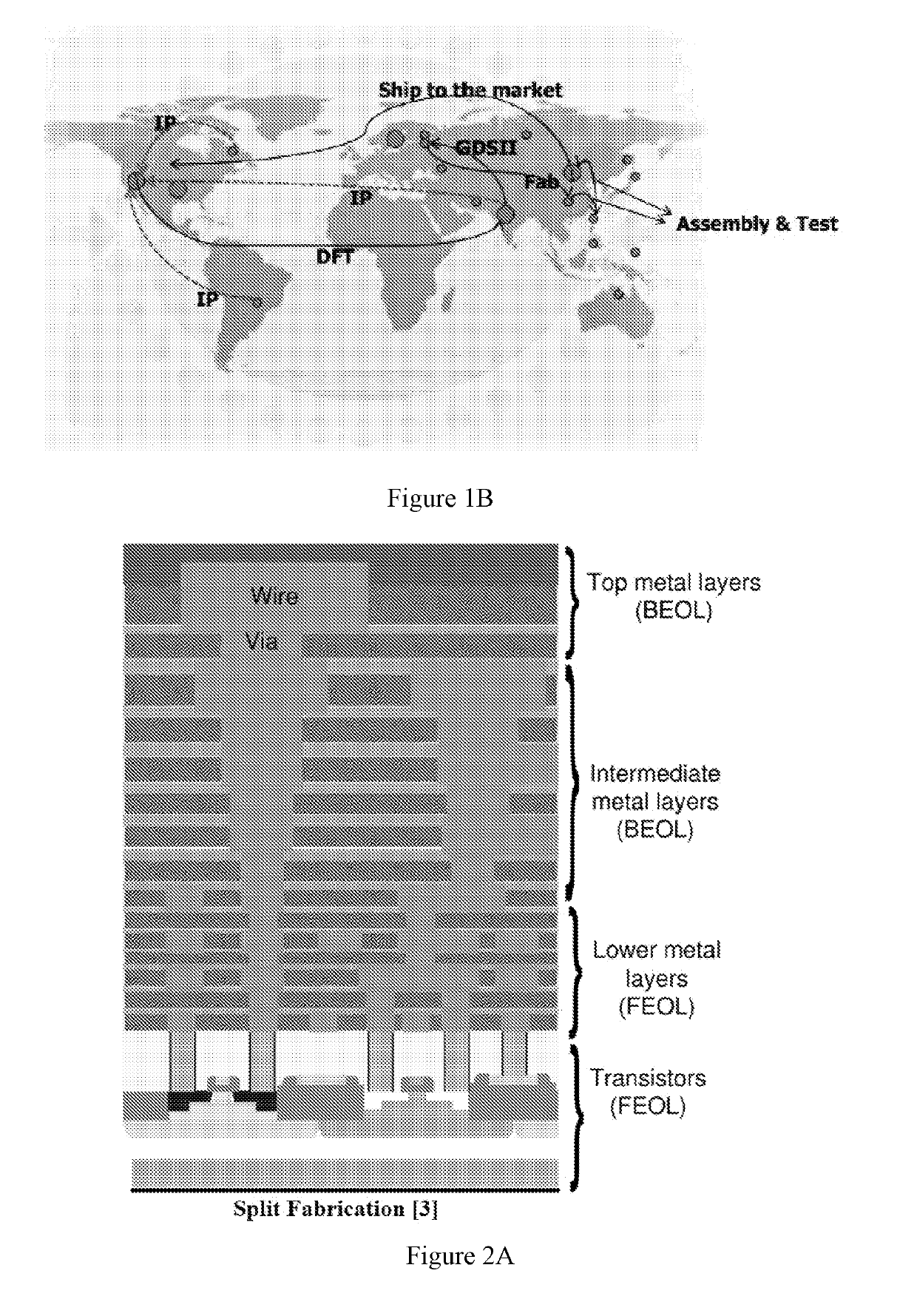
Under this divided business model, though the semiconductor company designing the IC can reduce the manufacturing costs and respond quickly to the market needs, the risk of security increases because the IC design company cannot control the whole process, particularly the manufacturing process.
However, these methods have considerable drawbacks in terms of design overhead, cost, and security.
Method used
View moreImage
Smart ImageViewing Examples

Examples
embodiment 1
[0037]A circuit comprising:
[0038]an original circuit configured to become an obfuscated circuit with a different output from the original circuit,
[0039]wherein the obfuscated circuit is configured to recover the output of the original circuit upon modification of the obfuscated circuit.
embodiment 2
[0040]The circuit according to embodiment 1, wherein the obfuscated circuit includes a logic gate, a rerouted connection, or both.
embodiment 3
[0041]The circuit according to embodiment 2, wherein the logic gate is at least one selected from an inverter, NAND, NOR, XOR, AND, and OR.
Login to View More PUM
 Abstract
Circuits and methods for protecting against intellectual property piracy and integrated circuit piracy from an untrusted third party are provided. A circuit can include an original circuit and an obfuscated circuit incorporated into the original circuit and changing the output of the original circuit, wherein the obfuscated circuit is configured to recover the output of the original circuit by modifying the obfuscated circuit. In addition, a method of manufacturing a semiconductor device can include designing a circuit including an original circuit and an obfuscated circuit, and fabricating the circuit, wherein the obfuscated circuit is configured to change an output of the original circuit and to recover the output of the original circuit by modifying the obfuscated circuit.
Description
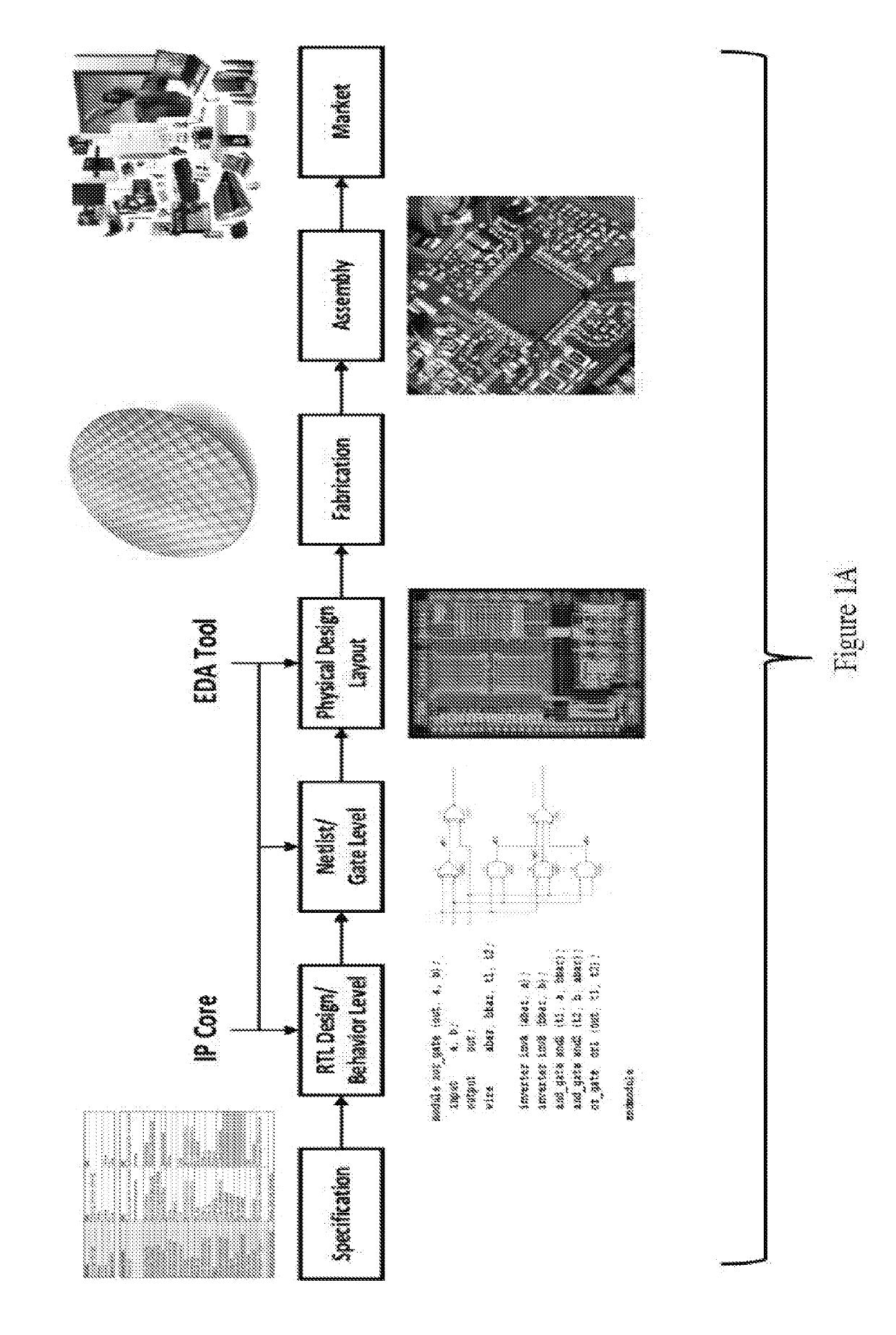
CROSS-REFERENCE TO A RELATED APPLICATION[0001]This application claims the benefit of U.S. Provisional Application Ser. No. 62 / 351,490, filed Jun. 17, 2016, the disclosure of which is hereby incorporated by reference in its entirety, including all figures, tables and drawings.GOVERNMENT SUPPORT[0002]This invention was made with government support under Grant No. FA9550-14-1-0351 awarded by Air Force Office of Scientific Research (AFSOR). The government has certain rights in the invention.BACKGROUND OF THE INVENTION[0003]The integrated circuit (IC) business scheme has changed over the last few decades as semiconductor scaling has reached a submicron level. A facility to manufacture a submicron semiconductor device requires an investment of several billion dollars, and this business condition leads to a division between semiconductor companies to design the IC and foundry companies to manufacture the IC designed by the semiconductor company. Under this divided business model, though th...
Claims
Login to View More Application Information
Patent Timeline
 Patent Type & AuthorityApplications(United States)
IPC IPC(8): G06F21/75G06F17/50
CPCG06F21/75G06F17/5077G06F21/76H01L23/573G06F21/14G06F30/333G06F30/327G06F30/39H01L21/762G06F30/394
InventorTEHRANIPOOR, MARK M.FORTE, DOMENIC J.SHAKYA, BICKYASADIZANJANI, NAVID
OwnerUNIV OF FLORIDA RES FOUNDATION INC