Method for manufacturing gallium nitride substrate using the hydride vapor phase epitaxy

a technology of nitride and hydride, which is applied in the direction of basic electric elements, electrical apparatus, semiconductor devices, etc., can solve the problems of reducing the crystallinity of nitride semiconductor substrates, cracks, and reducing the electrical characteristics of devices, so as to reduce the flow rate ratio of ammonia gas

a technology of nitride and hydride, which is applied in the direction of basic electric elements, electrical apparatus, semiconductor devices, etc., can solve the problems of reducing the crystallinity of nitride semiconductor substrates, cracks, and reducing the electrical characteristics of devices, so as to reduce the flow rate ratio of ammonia gas

US20190371597A1Active Publication Date: 2019-12-05IUCF HYU (IND UNIV COOP FOUND HANYANG UNIV)

Image

  • Method for manufacturing gallium nitride substrate using the hydride vapor phase epitaxy
  • Method for manufacturing gallium nitride substrate using the hydride vapor phase epitaxy
  • Method for manufacturing gallium nitride substrate using the hydride vapor phase epitaxy

Examples


example 1

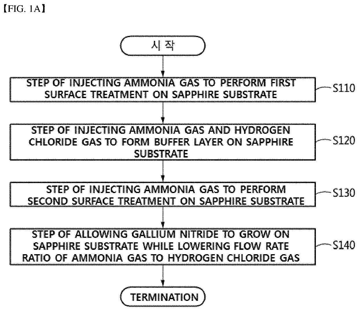
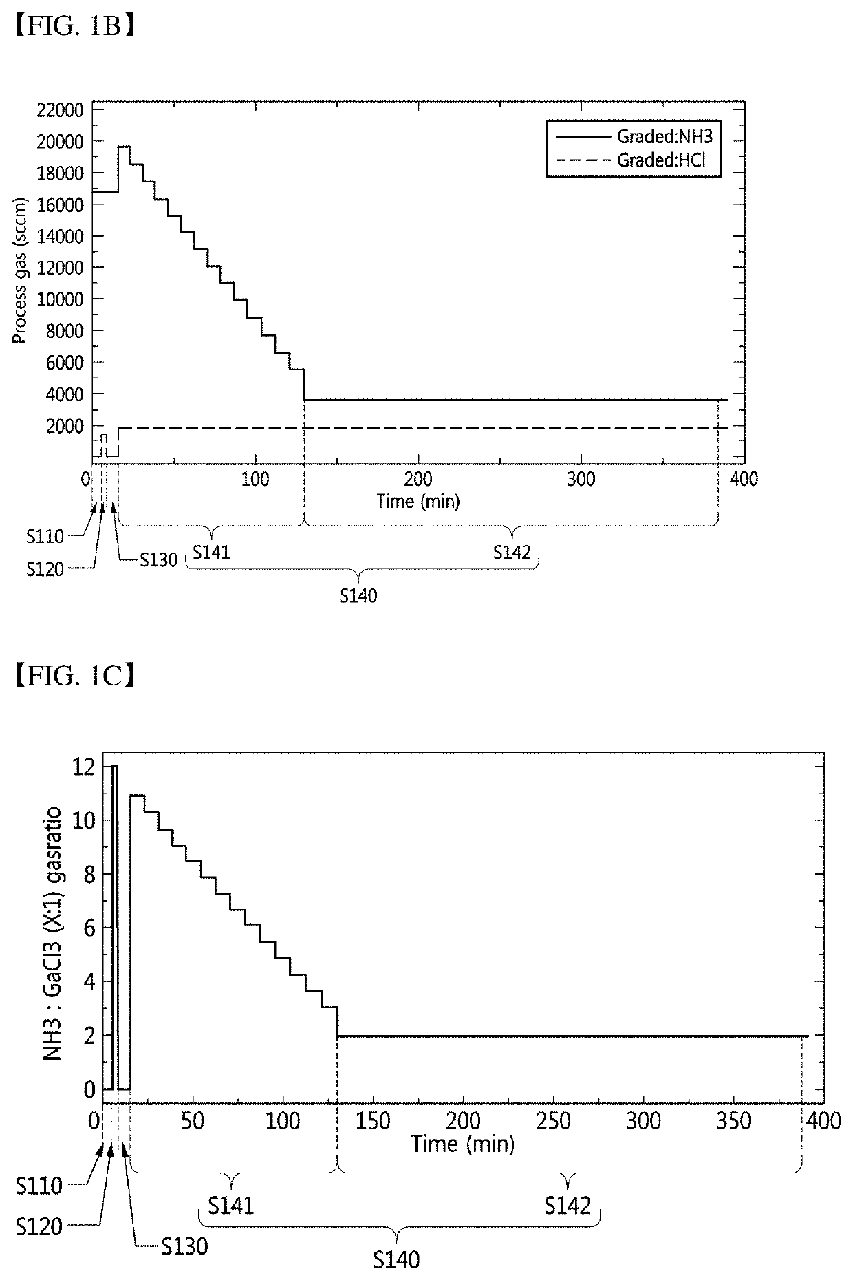
[0122]After a sapphire substrate was inserted into a hydride vapor phase growth reactor, the first surface treatment was performed at a temperature of 950° C. while ammonia gas was supplied, an aluminum nitride buffer layer was formed while ammonia gas and hydrogen chloride gas were supplied, and the second surface treatment was performed while ammonia gas was supplied again.

[0123]Next, gallium was placed in a gallium container included in the hydride vapor phase growth reactor, and hydrogen chloride gas was supplied while maintaining temperature at 850° C. to generate gallium chloride gas. Through another injection port, ammonia gas was supplied to the container set to a temperature of 950° C. while reducing the flow rate of ammonia gas stepwise (i.e., lowering the flow rate ratio (x:1) of ammonia gas to hydrogen chloride gas stepwise), so that gallium nitride having a thickness of about 300 μm was allowed to grow on a single crystal substrate.

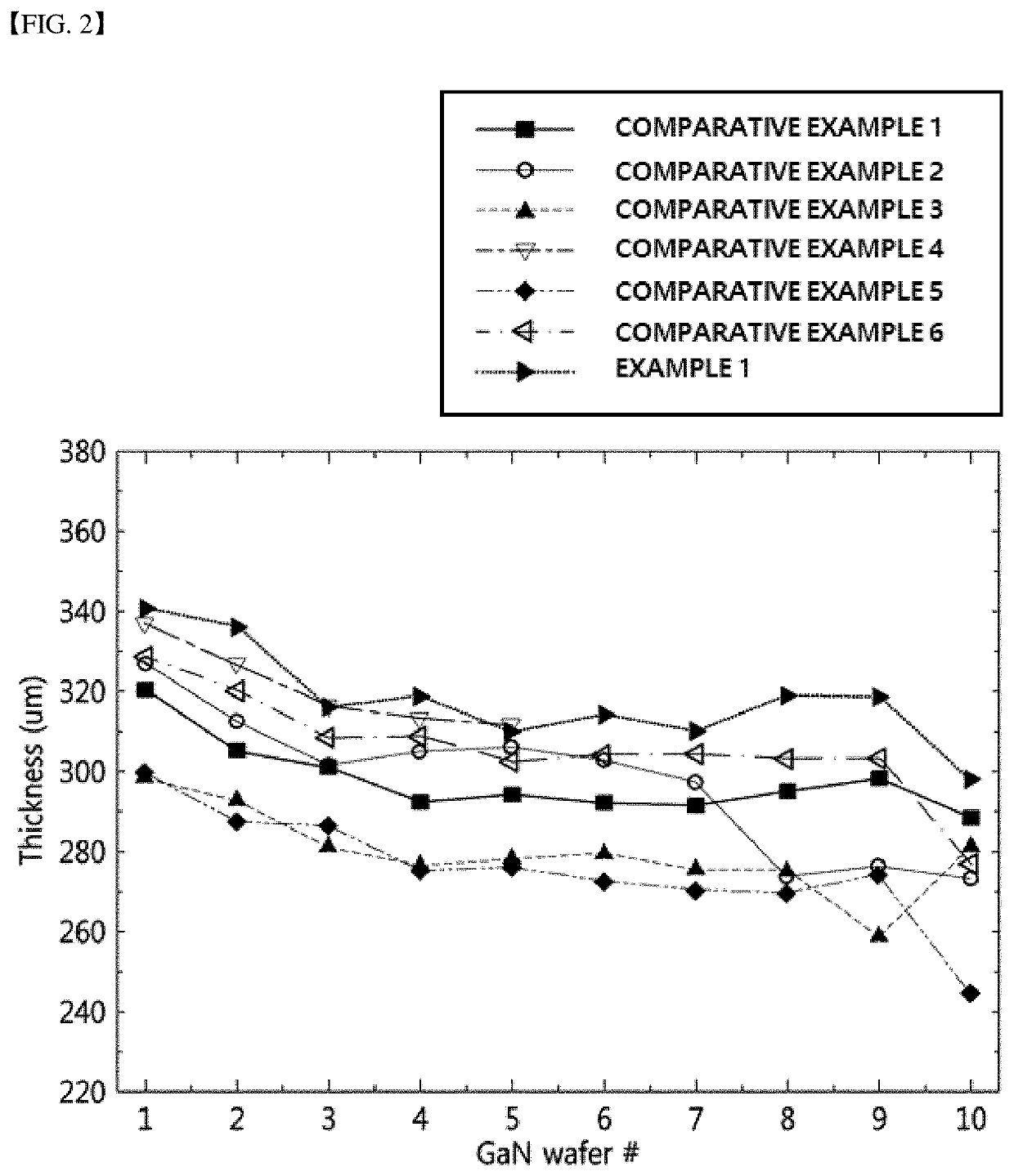
[0124]In addition, 10 gallium nitride ...


PUM


Abstract

Disclosed a method of fabricating a gallium nitride substrate using hydride vapor phase epitaxy (HVPE), including a step of injecting ammonia (NH3) gas to perform first surface treatment on a sapphire substrate; a step of injecting ammonia gas and hydrogen chloride (HCl) gas to form a buffer layer on the sapphire substrate; a step of injecting ammonia gas to perform second surface treatment on the sapphire substrate; and a step of allowing gallium nitride (GaN) to grow on the sapphire substrate while lowering the flow rate ratio of ammonia gas to hydrogen chloride gas stepwise.

Description

BACKGROUND OF THE DISCLOSUREField of the Disclosure[0001]The present disclosure relates to a method of fabricating a gallium nitride substrate using hydride vapor phase epitaxy (HVPE), and more particularly, to a method of fabricating a gallium nitride substrate having high quality and a low defect density by preventing bowing and cracking of the gallium nitride substrate.Description of the Related Art[0002]The performance and lifespan of semiconductor devices, such as laser diodes and light emitting diodes, are determined by various factors constituting the device, and are particularly affected by a base substrate on which elements are stacked. Several methods of fabricating a high quality semiconductor substrate have been proposed.[0003]A gallium nitride (GaN) substrate is a typical group III-V compound semiconductor substrate. In addition to a GaAs substrate and an InP substrate, the GaN substrate is suitably used for a semiconductor device. However, the fabrication costs of the ...

Claims


Application Information

Patent Timeline
05 Dec 2019
Publication
US20190371597A1
IPC
H01L21/02
CPC
H01L21/02458; H01L21/02639; H01L21/0242; H01L21/0254; H01L21/0262; H01L33/12; H01L33/32; H01L33/0075
Inventors
PARK, JEA GUN; SHIM, JAE HYOUNG