Manufacturing method of array substrate

Active Publication Date: 2019-12-19
AU OPTRONICS CORP
View PDF0 Cites 1 Cited by
  • Summary
  • Abstract
  • Description
  • Claims
  • Application Information

AI Technical Summary

Benefits of technology

The patent text describes a manufacturing method for an array substrate that reduces the use of photomasks, thereby decreasing manufacturing costs. This is achieved by using the same photomask for creating the first conductive layer and the third metal layer in the fan-out region. The technical effect is to make the manufacturing process more cost-effective and efficient.

Problems solved by technology

However, forming more conductive layers requires more photomasks and thus the manufacturing cost is increased.

Method used


Image

  • Manufacturing method of array substrate
  • Manufacturing method of array substrate
  • Manufacturing method of array substrate

Examples


Embodiment Construction

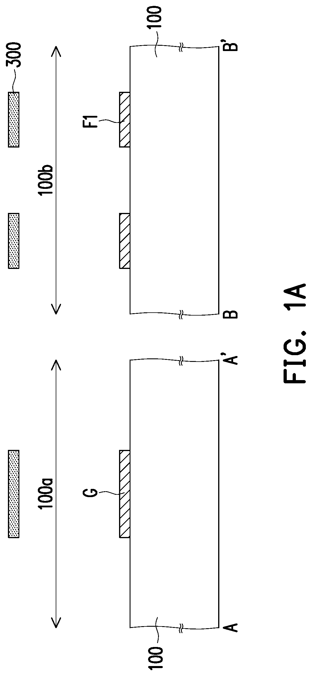
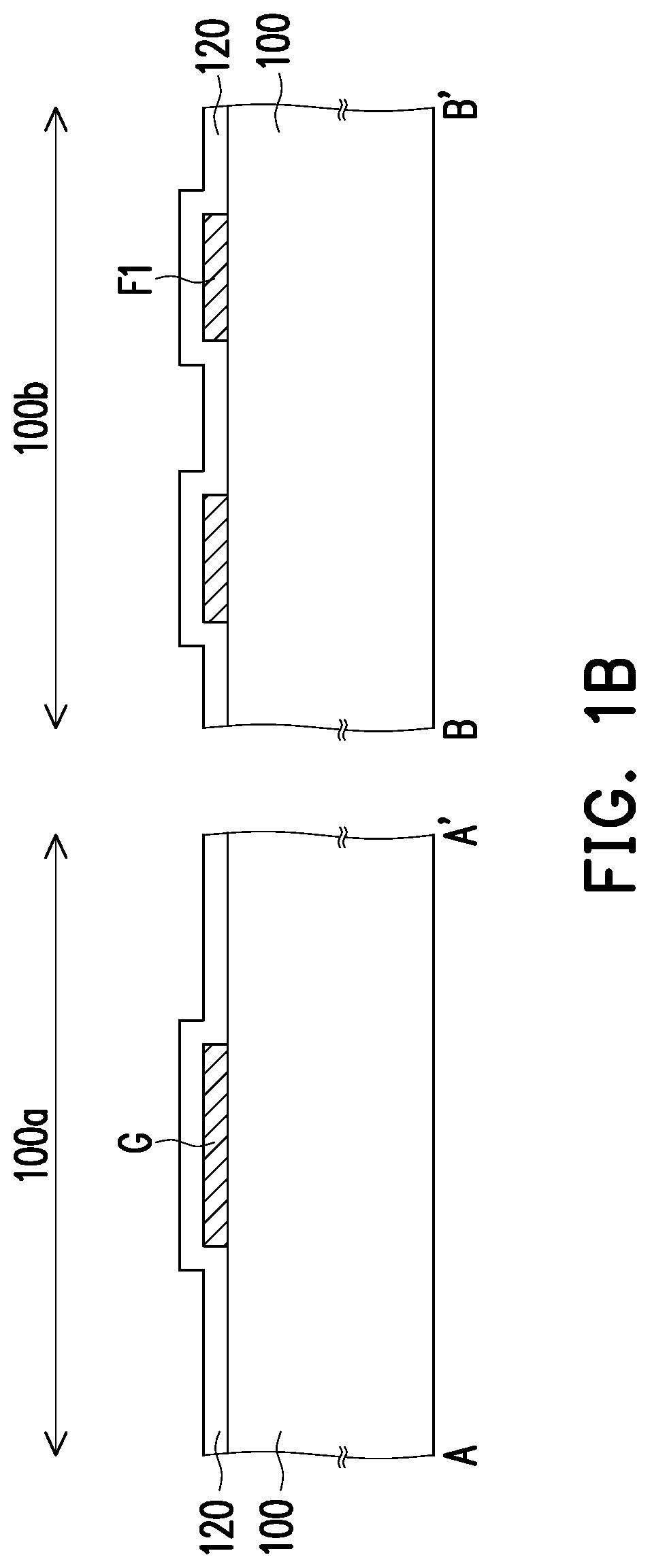
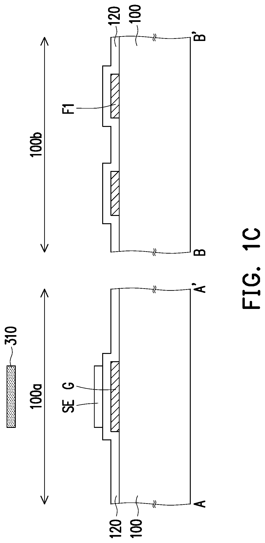
[0016]The invention is more comprehensively described with reference to the figures of the present embodiments. However, the invention may also be implemented in various different forms, and is not limited to the embodiments in the present specification. The thicknesses of the layers and regions in the figures are enlarged for clarity. The same or similar reference numerals represent the same or similar devices and are not repeated in the following paragraphs. Additionally, directional terminology, such as“top,”“bottom,”“left,”“right,”“front,” or “back,” etc., is used with reference to the orientation of the Figure(s) being described. As such, the directional terminology is used for purposes of illustration and is in no way limiting.

[0017]FIG. 1A to FIG. 10 are schematic cross-sectional views of a manufacturing method of an array substrate according to an embodiment of the disclosure. FIG. 2A, FIG. 3A and FIG. 4A are schematic top views of a pixel region of a manufacturing method of...


PUM


Abstract

A manufacturing method of an array substrate including following steps is provided. A plurality of scan lines are formed on a substrate having a pixel region and a fan-out region. A plurality of data lines are formed. A plurality of transistors are formed and respectively electrically connected to the corresponding scan lines and data lines. A plurality of common electrodes are formed. A plurality of pixel electrodes are formed and respectively electrically connected to the corresponding transistors. A plurality of first fan-out lines, second fan-out lines, and third fan-out lines are formed in the fan-out region. Each of the third fan-out lines includes a transparent conductive layer and an auxiliary conductive layer located on and contacting the transparent conductive layer. The third fan-out lines and the common electrodes are formed by the same photomask.

Description

CROSS REFERENCE TO RELATED APPLICATION[0001]This application claims the priority benefit of Taiwan application serial no. 107121013, filed on Jun. 19, 2018. The entirety of the above-mentioned patent application is hereby incorporated by reference herein and made a part of specification.BACKGROUNDField of the Disclosure[0002]The disclosure is related to a manufacturing method of an array substrate, and particularly to a manufacturing method of an array substrate of a display panel.Description of Related Art[0003]In recent years, there is a tendency that display panel is designed to have a reduced area of peripheral region of array substrate, and thus a portion of fan-out lines in the peripheral region needs to be changed into the form that different conductive layers are stacked onto each other to adapt to the reduced peripheral region. However, forming more conductive layers requires more photomasks and thus the manufacturing cost is increased.SUMMARY OF THE DISCLOSURE[0004]At leas...

Claims


Application Information

Patent Timeline
IPC IPC(8): H01L27/12H01L27/32G02F1/1345G02F1/1343
CPCH01L27/1288H01L27/3276H01L27/3262H01L27/1262H01L27/1218G02F1/13439G02F1/13458G02F1/13338G02F1/134363G02F1/13452G02F1/1362G02F1/136286G02F1/13456H01L27/124H01L27/1259G02F1/13629H10K59/1213H10K59/131
Inventor HSU, WEN-YICHEN, PEI-MINGCHEN, MAW-SONG
Owner AU OPTRONICS CORP
Why Eureka
Try Eureka