Three-dimensional semiconductor memory device

Active Publication Date: 2019-12-26
SAMSUNG ELECTRONICS CO LTD
View PDF2 Cites 22 Cited by
  • Summary
  • Abstract
  • Description
  • Claims
  • Application Information

AI Technical Summary

Problems solved by technology

However, a high-cost equipment is required for such a fine pattern formation in a 2D or planar semiconductor ma

Method used


Image

  • Three-dimensional semiconductor memory device
  • Three-dimensional semiconductor memory device
  • Three-dimensional semiconductor memory device

Examples


Embodiment Construction

[0018]Various example embodiments will now be described more fully with reference to the accompanying drawings in which some example embodiments are shown. However, the inventive concepts may be embodied in many alternate forms and should not be construed as limited to only example embodiments set forth herein.

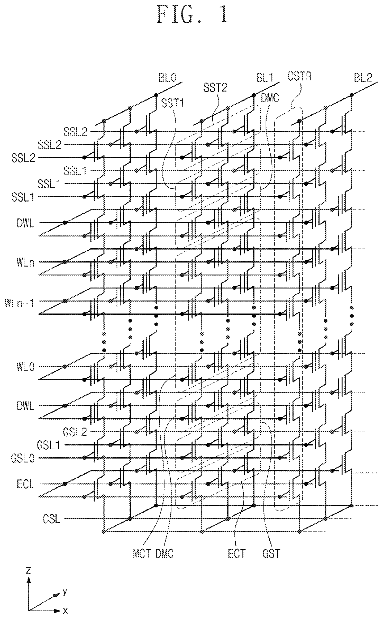
[0019]FIG. 1 is a schematic circuit diagram illustrating a cell array of a three-dimensional semiconductor memory device according to example embodiments.

[0020]Referring to FIG. 1, a three-dimensional (3D) semiconductor memory device may include a common source line CSL, a plurality of bit lines BL0-BL2, and / or a plurality of cell strings CSTR between the common source line CSL and the bit lines BL0-BL2. The plurality of cell strings CSTR may be connected in parallel to each of the bit lines BL0-BL2. The cell strings CSTR may be connected in common to the common source line CSL. For example, the cell strings CSL may be disposed between the bit lines BL0-BL2 and one common sour...


PUM


Abstract

A three-dimensional semiconductor memory device includes a substrate, an electrode structure including gate electrodes sequentially stacked on the substrate, a source structure between the electrode structure and the substrate, vertical semiconductor patterns passing through the electrode structure and the source structure, a data storage pattern between each of the vertical semiconductor patterns and the electrode structure, and a common source pattern between the source structure and the substrate. The common source pattern has a lower resistivity than the source structure and is connected to the vertical semiconductor patterns through the source structure.

Description

CROSS-REFERENCE TO RELATED APPLICATION[0001]This application claims priority under 35 U.S.C. § 119 to Korean Patent Application No. 10-2018-0071518 filed on Jun. 21, 2018 in the Korean Intellectual Property Office, the disclosure of which is hereby incorporated by reference in its entirety.TECHNICAL FIELD[0002]Example embodiments of the present disclosure relate to a semiconductor memory device, and more specifically, to a three-dimensional semiconductor memory device including memory cells arranged three-dimensionally.DISCUSSION OF RELATED ART[0003]A semiconductor device is highly integrated to meet demands of high performance and low costs. For example, an integration degree of a two-dimensional (2D) or planar semiconductor device is mainly determined by an area used for a unit memory cell. Therefore, the integration density of the 2D or planar semiconductor device depends on a technique used for a fine pattern formation. However, a high-cost equipment is required for such a fine ...

Claims


Application Information

Patent Timeline
IPC IPC(8): H01L27/11582H01L27/11565H01L27/1157H01L27/11573H01L21/28H01L29/423H01L23/522
CPCH01L29/40117H01L27/11565H01L27/11573H01L27/11582H01L27/1157H01L27/11556H01L27/11524H01L29/42344H01L27/11526H01L29/42328H01L27/11519H01L23/5226H10B41/35H10B41/27H10B43/35H10B43/27H10B43/40H10B41/41H10B43/10H10B41/10H10B41/40
Inventor LIM, GEUNWONHONG, SANGJUNBAEK, SEOKCHEON
Owner SAMSUNG ELECTRONICS CO LTD
Why Eureka
Try Eureka