

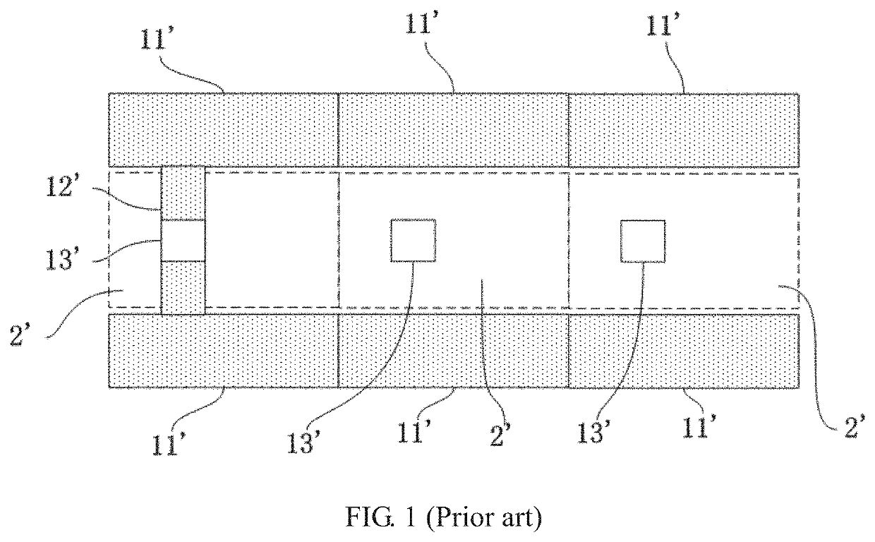
Display panel and manufacturing method for the same
a technology for display panels and manufacturing methods, applied in the field of display panels, can solve the problems of easy cracking of the risk that the main region spacer will not reach the desired heigh
- Summary
- Abstract
- Description
- Claims
- Application Information
AI Technical Summary
Benefits of technology
Problems solved by technology
Method used
Image

Examples
Embodiment Construction
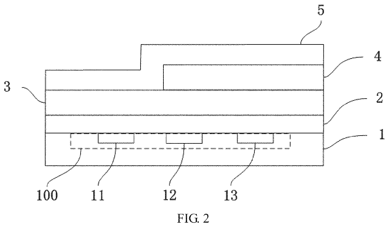
[0035]The present invention provides a display panel, as shown in FIG. 2, the display panel includes: an array substrate 1, a passivation layer 2 on the array substrate 1, an organic planarization layer 5 on the passivation layer 2. The display panel further includes a first color resist layer 3 and a second color resist layer 4, the first color resist layer 3 and the second color resist layer 4 are damped between the passivation layer 2 and the organic planarization layer 5. The pixel structure in the present invention may be a 3T pixel structure, that is, each sub-pixel circuit includes three thin-film transistors.
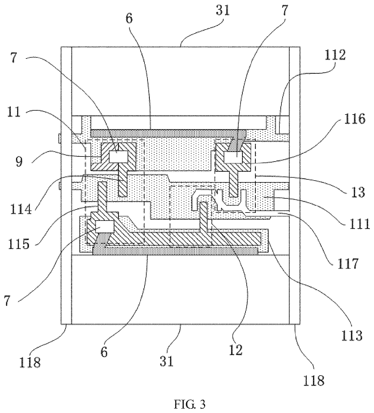
[0036]The array substrate 1 includes multiple sub-pixel circuits 100, and each sub-pixel circuit 100 includes at least two thin-film transistors, for example, three thin-film transistors 11, 12, and 13 shown in FIG. 2. At least two via holes 7 as shown in FIG. 3, for example, three via holes are prepared on the passivation layer 2 and the organic planarization layer 5 ab...
PUM
| Property | Measurement | Unit |
|---|---|---|
| transmittance | aaaaa | aaaaa |
| semi-transparent | aaaaa | aaaaa |
| stability | aaaaa | aaaaa |
Abstract
Description
Claims
Application Information