Apparatus for and method of manufacturing an article using photolithography and a photoresist
a technology of photolithography and photoresist, which is applied in the direction of electrical equipment, basic electric elements, instruments, etc., can solve the problems of large processing plant requirements, large time and expense, and inability to produce free-standing parts, and achieve the production of free-standing parts. , to achieve the effect of rapid printing of microstructures, and rapid printing of self-powered sensors
- Summary
- Abstract
- Description
- Claims
- Application Information
AI Technical Summary
Benefits of technology
Problems solved by technology
Method used
Image

Examples
example 1
Microstructures
[0320]These examples demonstrate semi-aligned multilayer textured surfaces, made up of two or more layers, which may include a substrate; which may be one or more layers of photoresist, or may be another material such as a polymer or paper, or may be substrateless (free-standing).
[0321]These examples can all be manufactured on a single layer device, such as described in Apparatus Example 1.
[0322]1a) Micro-Textured Surfaces
[0323]This example, with reference to FIG. 39, describes printing a “Shark's skin” type of geometric repeated pattern, which may be used for lubrication, antifouling surfaces, or for high surface area structures for catalysis, for example.
[0324]The example was patterned from a custom script designed in CleWin5, and printed in EMS DF 3550, a 50 μm thick negative dry resist, using a wholly exposed bottom layer as a substrate, with a top micropatterned layer.
[0325]The pattern is exposed with a print mask of 3386 dpi (7 μm) resolution (Agfa HNS polyester...
example 2
Greyscale Channel
[0342]Greyscale microfluidics channels have a use in that they can form rounded walls, so as to avoid reducing the laminar microfluidic flow as seen in conventional rectangular section channels with a 90° angle.
[0343]This example, with reference to FIG. 45, is made of two layers including a substrate and tapered sidewalls. The channel was made in 50 μm thick DF-3550 resist laminated onto a polymethyl methacrylate (Perspex) substrate using a Sky 335R6 Pouch Laminator set at 27° C. and using the lowest speed setting. The image was projected with a Texas Instruments DLPDLCR4710EVM-G2 DLP projector (with a 395 nm LED, and InfiniGage main body lens from Edmund optics) and a custom greyscale bitmap pattern for 3 minutes.
[0344]After exposure, the channel was cured for 10 minutes at 100° C. on an Electronic Microsystems hotplate, then cooled and developed for 6 minutes in PGMEA.
example 3
High Resolution Prints
[0345]This example, with reference to FIG. 46, demonstrates a collection of high resolution 10 μm sided printed bridges.
[0346]The bridges were manufactured in EMS DF 3510, 10 μm thick negative dry resist film. Three layers were used: a base layer and two pattern layers. The base layer was wholly exposed (no pattern) with a 5 mW / cm2 collimated mercury arc lamp for the source, and an exposure time of 1 minute. Both pattern layers used a prepatterned custom chrome mask photoplate and the 5 mW / cm2 collimated mercury arc lamp with a 30 second exposure. After exposing each layer it was laminated to the previous layer with a Sky 335R6 Pouch Laminator set at 50° C. and using the lowest speed setting. An Electronic Microsystems hotplate was used to cure the structures at 100° C. for 10 minutes before removing uncross-linked material by dissolving in PGMEA for 6 minutes.
PUM
| Property | Measurement | Unit |
|---|---|---|
| sizes | aaaaa | aaaaa |
| sizes | aaaaa | aaaaa |
| sizes | aaaaa | aaaaa |
Abstract
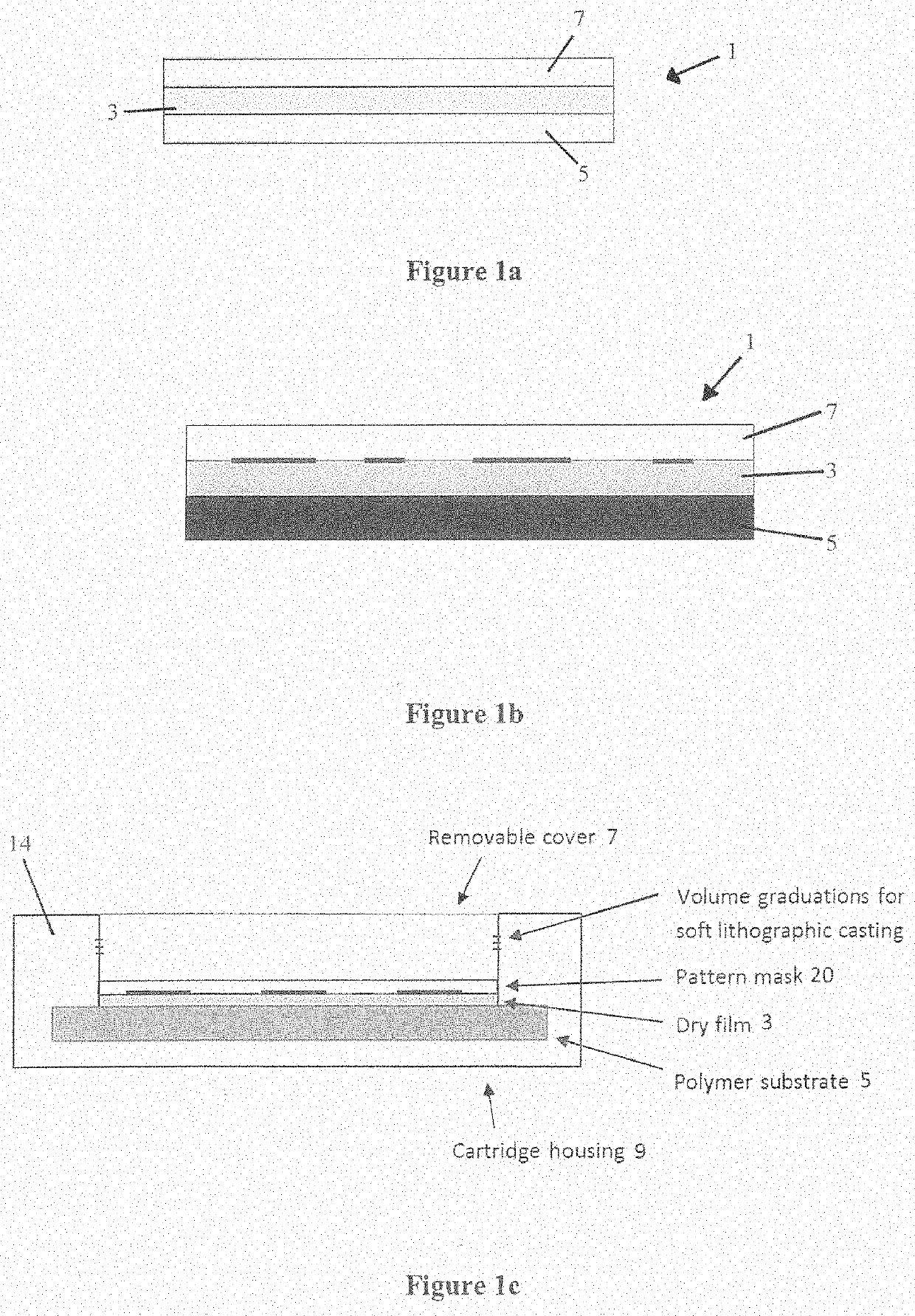
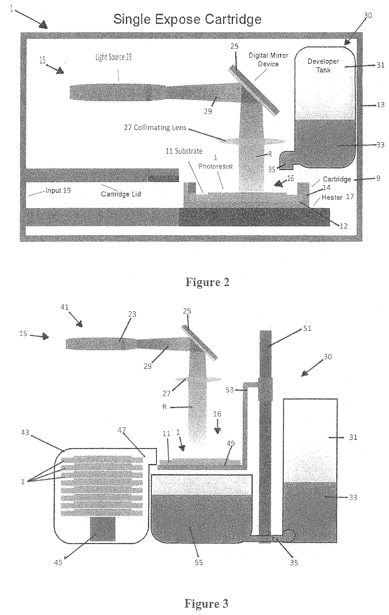
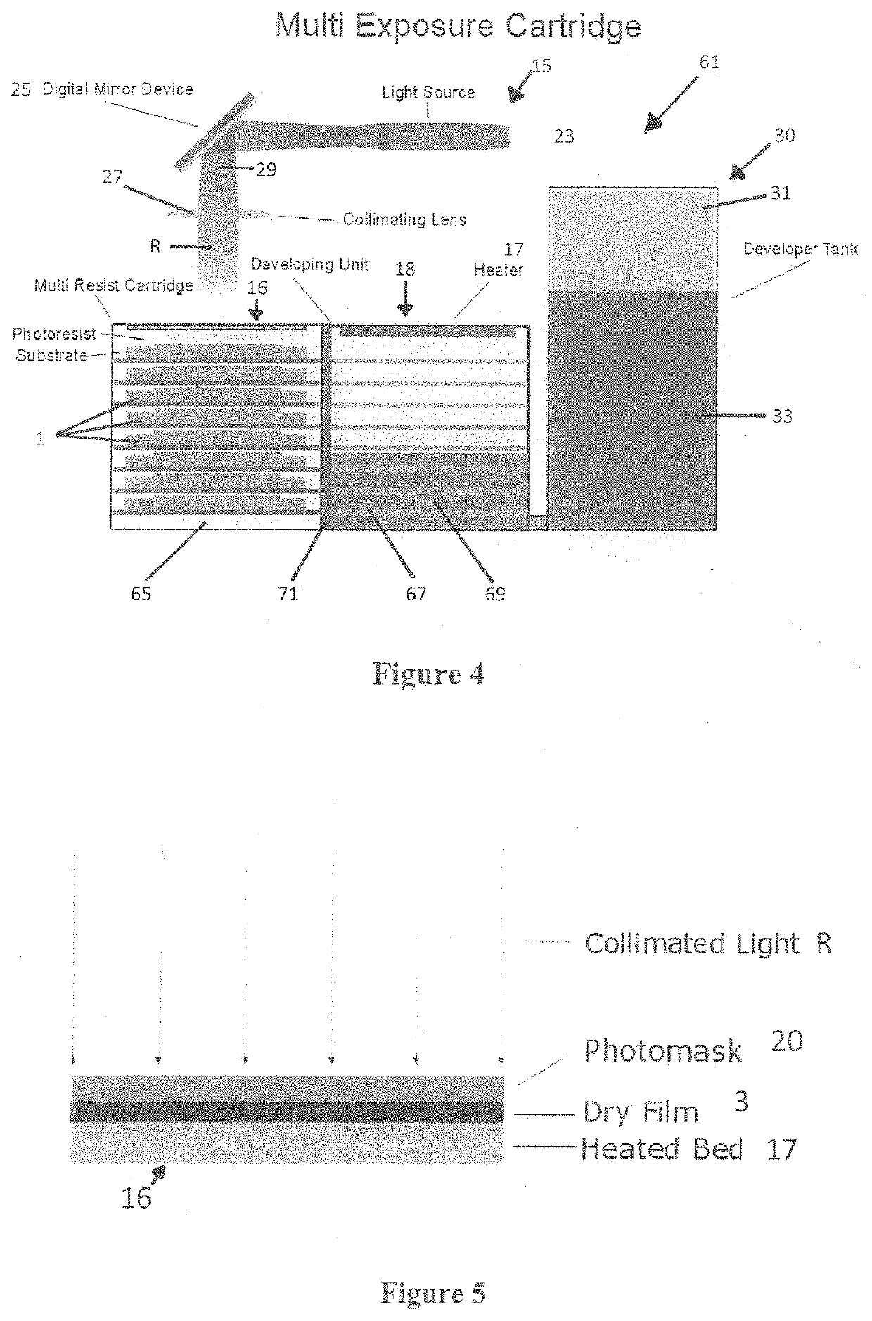
- a. a housing configured to receive the photoresist and locate the photoresist in at least one operational position in the housing;
- b. an exposure system configured to emit radiation which is incident on the photoresist material when in the operational position, to induce a change in one or more properties of the area(s) of the photoresist material exposed to the radiation; and
- c. a heater configured to heat the photoresist material to cure the photoresist material to the substrate when the photoresist is in the operational position, or is in a different operational position in the housing; wherein
- d. the housing is radiation excluding such that external radiation cannot enter the housing at least to the extent that the external radiation is sufficiently excluded from the housing to prevent, or minimise polymerisation of the photoresist material, and further wherein the housing is a clean housing configured to prevent unwanted contamination from entering the housing, at least when the photoresist is located in the or each operational position.
Description
Claims
Application Information
 - R&D Engineer
- R&D Manager
- IP Professional
- Industry Leading Data Capabilities
- Powerful AI technology
- Patent DNA Extraction
Browse by: Latest US Patents, China's latest patents, Technical Efficacy Thesaurus, Application Domain, Technology Topic.
© 2024 PatSnap. All rights reserved.Legal|Privacy policy|Modern Slavery Act Transparency Statement|Sitemap