
Method for etching recessed structures

Active Publication Date: 2020-05-28
MURATA MFG CO LTD
View PDF0 Cites 0 Cited by
  • Summary
  • Abstract
  • Description
  • Claims
  • Application Information

AI Technical Summary

Benefits of technology

This patent allows for the simultaneous recessing of multiple micromechanical structures in the same layer without using a separate mask for each recess area. This is possible because the method protects the vertical sidewalls formed in the first deep etch with a self-supporting etching mask before the second deep etching step. The result is the creation of multiple recess depths without damaging the micromechanical structures.

Problems solved by technology

Irregularities in patterned micromechanical structures can introduce measurement errors or cause short-circuits which entirely prevent measurement or actuation in the MEMS device.

Method used


Image

  • Method for etching recessed structures
  • Method for etching recessed structures
  • Method for etching recessed structures

Examples


Embodiment Construction

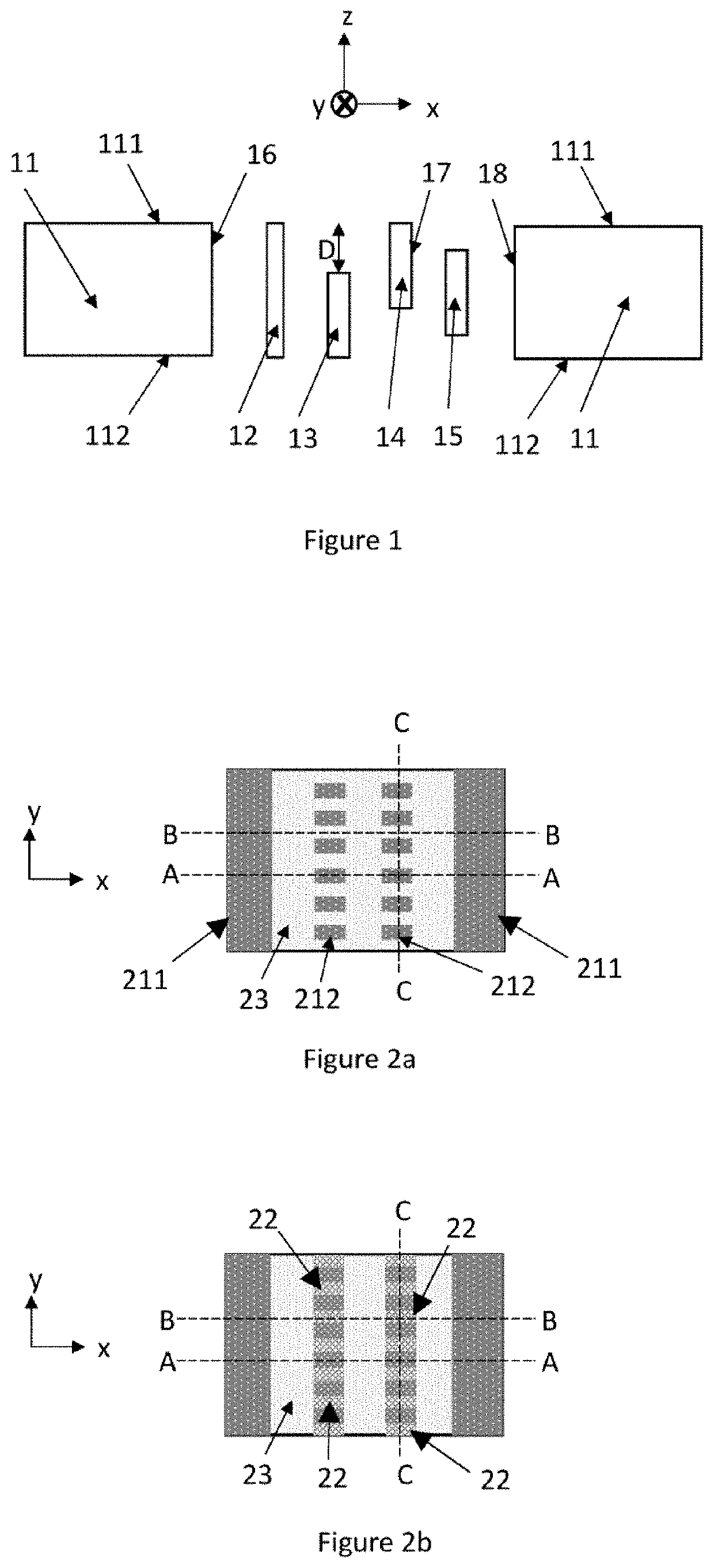
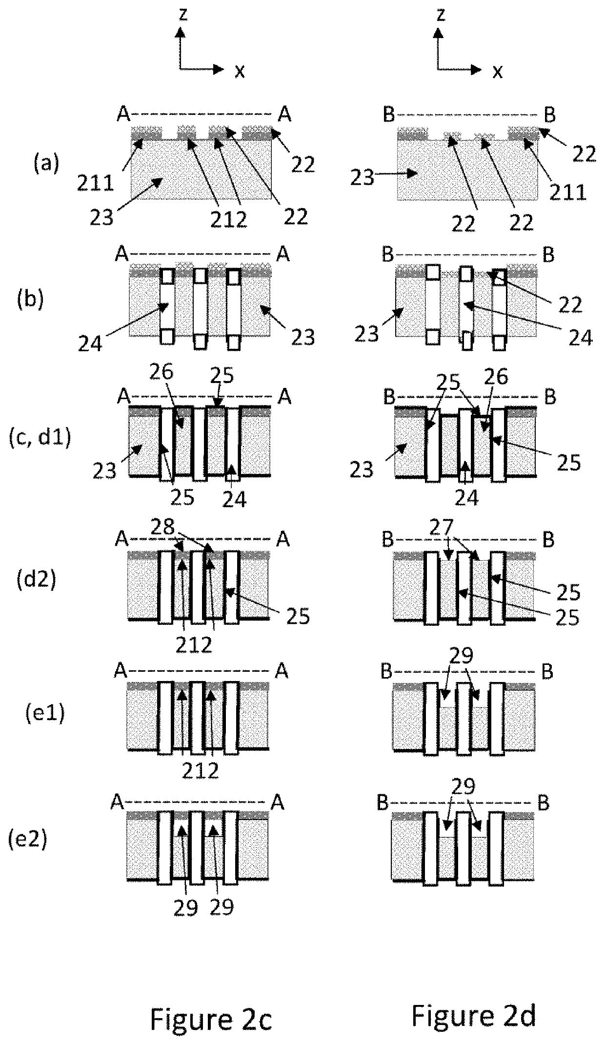
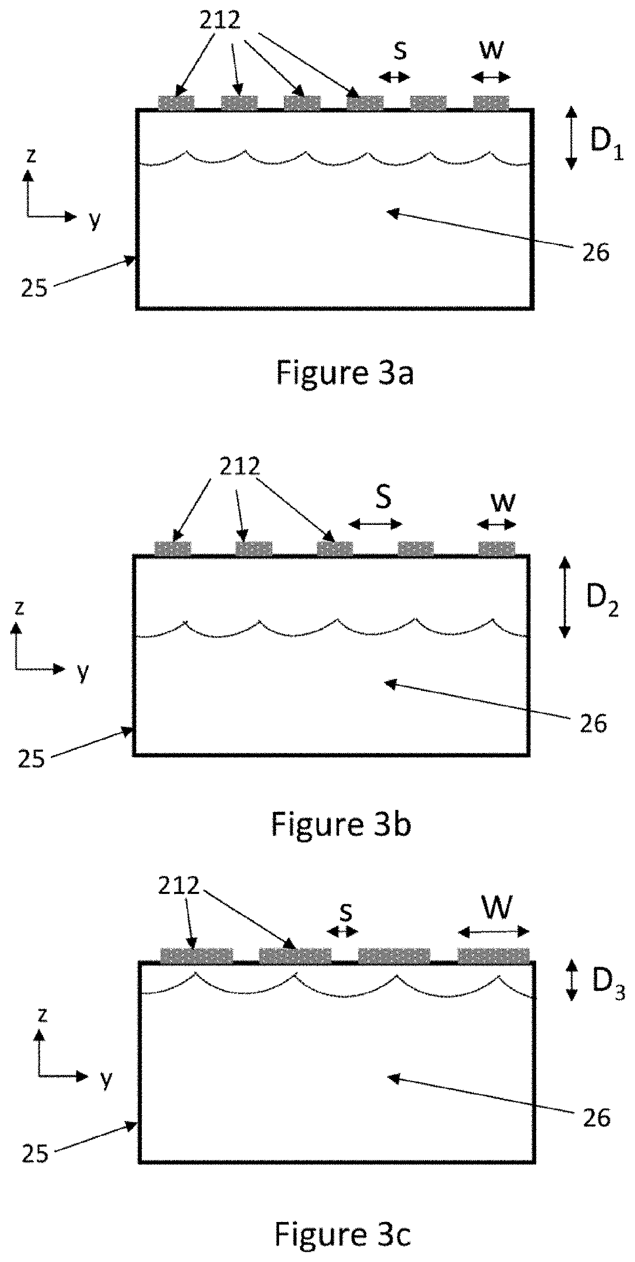
[0023]This disclosure describes a method for manufacturing micromechanical structures in a structural layer of a wafer. The manufactured structures include at least one recess area where the micromechanical structures are vertically recessed in relation to a horizontal face of the structural layer. The method comprises the following steps a-e:[0024]a) depositing and patterning a first etching mask and a second etching mask on the horizontal face of the structural layer, wherein the first etching mask is deposited before the second etching mask, and the second etching mask defines at least one recess area which corresponds to at least one structure which is to be vertically recessed, and the first etching mask defines at least one etch-control area within the at last one recess area, so that each etch-control area is separated from other etch-control areas and extends across the at least one recess area, from one side of said recess area to another side of said recess area,[0025]b) e...


PUM


Abstract

A method for manufacturing recessed micromechanical structures in a wafer. A first etching mask and a second etching mask are patterned on the horizontal face of the wafer. The second etching mask defines at least one recess area and the first etching mask defines at least one etch-control area within the at least one recess area. The placement, number and dimensions of the etch-control areas influence the vertical etch rate of the recessed structure. Adjacent structures can be etched to different recess depths by selecting suitable etch-control areas.

Description

FIELD OF THE DISCLOSURE[0001]The present disclosure relates to micromechanical devices, and more particularly to etching methods for manufacturing micromechanical device layers in a device wafer.BACKGROUND OF THE DISCLOSURE[0002]Microelectromechanical (MEMS) systems often comprise micromechanical parts formed in the structural layer of a device wafer by etching. Micromechanical parts with suitable dimensions can form partly mobile structures supported by the surrounding parts of the structural layer. MEMS systems which comprise partly mobile micromechanical structures include, for example, acceleration sensors, gyroscopes, micromirrors, optical switches and scanners.[0003]Irregularities in patterned micromechanical structures can introduce measurement errors or cause short-circuits which entirely prevent measurement or actuation in the MEMS device. Accurate etching is therefore an important part of MEMS manufacturing processes.[0004]This disclosure relates to etching of structural l...

Claims


Application Information

Patent Timeline
IPC IPC(8): H01L21/308H01L21/306
CPCH01L21/30608H01L21/3081B81C1/0015
Inventor FUJII, HIDETOSHI
Owner MURATA MFG CO LTD
Learn More