Flexible display panel and manufacturing method thereof

a display panel and flexible technology, applied in the field of touch display devices, can solve the problem of not being able to achieve a narrower border, and achieve the effect of reducing the width of the trace in the edge, no additional space, and reducing the non-display area

Active Publication Date: 2020-06-04
WUHAN CHINA STAR OPTOELECTRONICS SEMICON DISPLAY TECH CO LTD
View PDF0 Cites 0 Cited by
  • Summary
  • Abstract
  • Description
  • Claims
  • Application Information

AI Technical Summary

Benefits of technology

[0024]In comparison to the prior art, the present disclosure has advantages that the present disclosure provides a flexible display panel and a manufacturing method thereof, in which a traditional trace position is changed, and a hidden trace design is adopted. The trace and a display area are designed in the same position, so that no additional space is occupied, and a non-display area is reduced, thereby effectively reducing a width of the trace in an edge of a panel. It can even achieve zero edge width, increase a screen-to-body ratio, and reduce materials used in the same size. Furthermore, touch and display are integrated to achieve a narrow border solution, and a bonding area can also achieve a very narrow border.

Problems solved by technology

In order to achieve a narrow border, a touch screen currently employs an edge trace, but when minimum line width of the trace reaches the limit of process, it is impossible to continue to achieve a narrower border.

Method used


Image

  • Flexible display panel and manufacturing method thereof
  • Flexible display panel and manufacturing method thereof
  • Flexible display panel and manufacturing method thereof

Examples


first embodiment

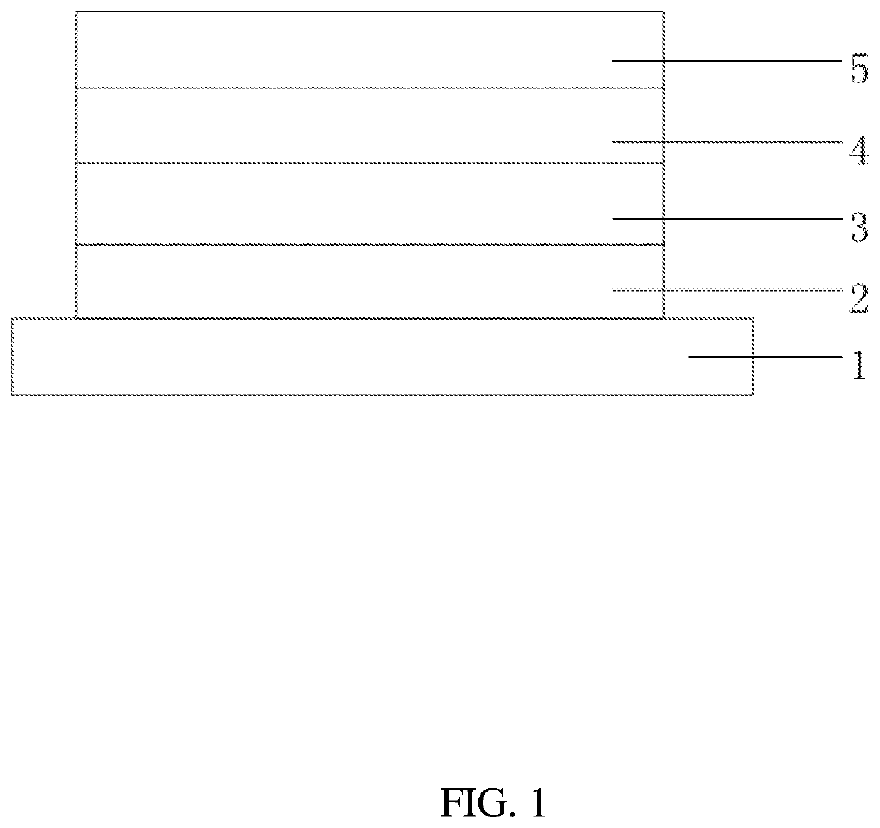
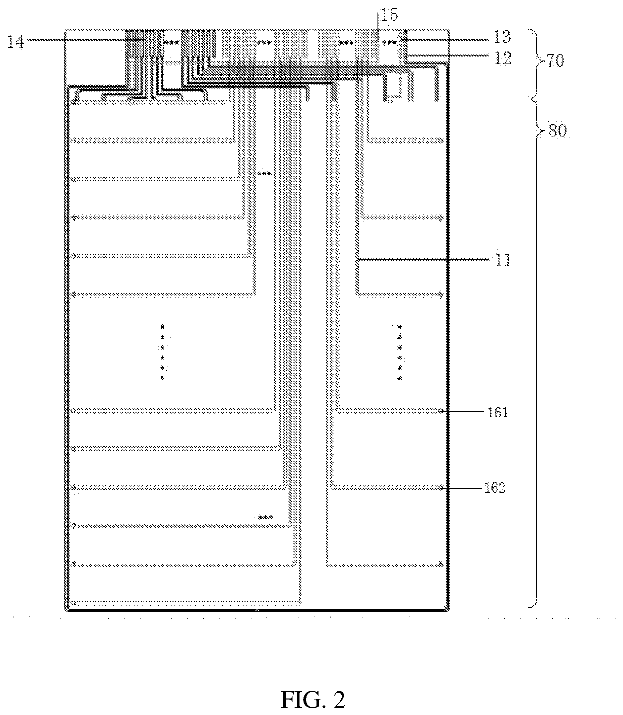
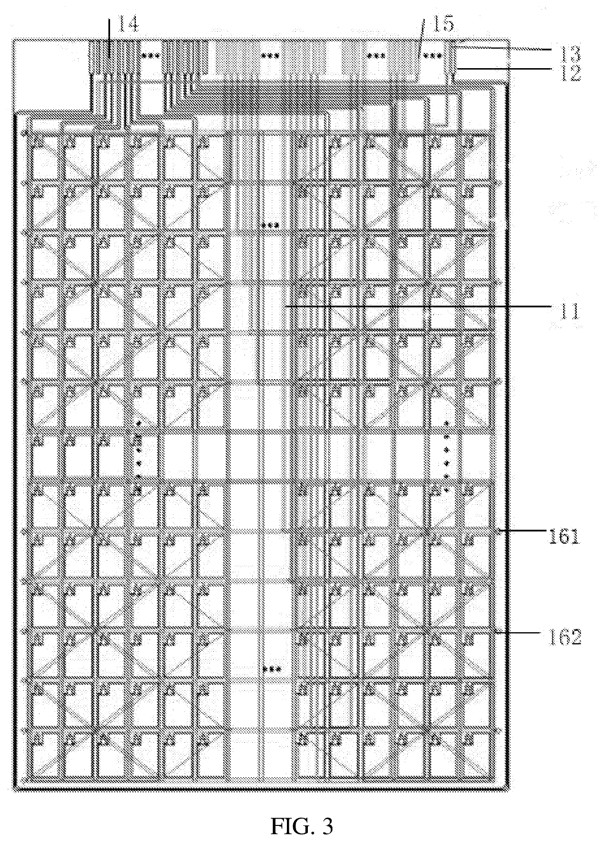
[0038]Referring to FIG. 1, FIG. 2, and FIG. 3, the present provides a flexible display panel defining a display area, a bonding area, and a border area. The flexible display panel includes a flexible substrate 1, a protective layer 2, a semiconductor layer 3, a light-emitting layer 4, and a touch layer 5.

[0039]The flexible substrate 1 corresponding to the display area is provided with a gate lead trace 11, a ground trace 12, a touch sensor receiving electrode lead trace 13, and a display area pad 80. The protective layer 2 corresponding to the border area is provided with a first through hole 161 and a second through hole 162. The gate lead trace 11 is electrically connected to a gate of the semiconductor layer 3 through the first through hole 161. The touch sensor receiving electrode lead trace 13 is electrically connected to a touch sensor receiving electrode on the touch layer 5 through the second through hole 162.

[0040]The protective layer 2 is an electrically insulating layer t...

second embodiment

[0042]Referring to FIG. 1, FIG. 4, and FIG. 5, the present also provides a flexible display panel defining a display area, a bonding area, and a border area. The flexible display panel includes a flexible substrate 1, a protective layer 2, a semiconductor layer 3, a light-emitting layer 4, and a touch layer 5.

[0043]The flexible substrate 1 corresponding to the display area is provided with a gate lead trace 21, a ground trace 22, a touch sensor receiving electrode lead trace 23, a data lead trace 24, a touch sensor transmitting electrode lead trace 25, and a display area pad 80. An end of the protective layer 2 corresponding to the border area is provided with a first through hole 261, a second through hole 262, a third through hole 263, and a fourth through hole 264. The gate lead trace 21 is electrically connected to a gate of the semiconductor layer 3 through the first through hole 261. The touch sensor receiving electrode lead trace 23 is electrically connected to a touch sensor...

third embodiment

[0045]Referring to FIG. 6, the present disclosure also provides a manufacturing method of a flexible display panel, which includes following steps.

[0046]In step S11, a gate lead trace 11, a ground trace 12, a touch sensor receiving electrode lead trace 13, and a display area pad 80 are formed on a flexible substrate 1 corresponding to a display area.

[0047]In step S12, a protective layer 2 is formed on the flexible substrate 1, and a first through hole 161 and a second through hole 162 are formed on an edge of the protective layer 2 corresponding to a border area.

[0048]The protective layer 2 is an electrically insulating layer that protects all traces on flexible substrate 1.

[0049]In step S13, a semiconductor layer 3 and a bonding area pad 70 are formed, and a data lead trace 14 is simultaneously formed, and the gate lead trace 11 is electrically connected to a gate of the semiconductor layer 3 through the first through hole 161.

[0050]The gate lead trace 11, the ground trace 12, and ...


PUM

PropertyMeasurementUnit
flexibleaaaaaaaaaa
electrically insulatingaaaaaaaaaa
areaaaaaaaaaaa

Abstract

A flexible display panel is provided, defining a display area, a bonding area, and a border area, and including a flexible substrate, a protective layer, a semiconductor layer, and a touch layer. A gate lead trace, a ground trace, a touch sensor receiving electrode lead trace, and a display area pad are disposed on the flexible substrate corresponding to the display area. The protective layer corresponding to the border area is provided with a first through hole, and the gate lead trace is electrically connected to a gate of the semiconductor layer through the first through hole. The disclosure has advantages of changing a traditional trace position, adopting a hidden trace design, and designing the trace in the same position as the display area, so that no additional space is occupied, and a non-display area is reduced, thereby effectively reducing a trace width in an edge of a panel.

Description

FIELD OF DISCLOSURE[0001]The present disclosure relates to the field of touch display devices, and in particular, to a flexible display panel and a manufacturing method thereof.BACKGROUND[0002]In recent years, with increasing use of consumer electronic products, more and more products have been applied by combining touch functions with displays. Touch technology has become a popular development technology because of its convenient operation and high integration.[0003]The touch technology has developed rapidly in recent years, and a variety of touch technologies have been employed in mass production. For a current touch display panel, according to a position of a touch sensor, the touch sensor can be classified as an on-cell (the touch sensor covers a liquid crystal cell), an in-cell (the touch sensor is embedded in the liquid crystal cell), and an out-cell (the touch sensor is externally mounted on the display panel).[0004]With advancement of technology, people are increasingly dema...

Claims


Application Information

Patent Timeline
Patent Type & Authority Applications(United States)
IPC IPC(8): G06F1/16G02F1/1333G02F1/1362G02F1/1335G02F1/1339
CPCG02F1/1339G02F1/136286G02F2001/136295G02F1/133305G06F1/1652G06F1/1643G02F1/133528G02F1/13338G06F3/0412G02F1/136295
Inventor FENG, XIAOLIANG
Owner WUHAN CHINA STAR OPTOELECTRONICS SEMICON DISPLAY TECH CO LTD
Why Eureka
Try Eureka