Methods for forming multilayer horizontal nor-type thin-film memory strings

a memory string and multi-layer technology, applied in the direction of basic electric elements, electrical equipment, semiconductor devices, etc., can solve the problems of increasing the cost-per-bit, snaking, twisting, bowing or shortening between adjacent active strips, and more silicon real estate per bit, so as to achieve a wider, mechanically stable, and less challenging active strip. , the effect of superior scaling

Active Publication Date: 2020-06-04
SUNRISE MEMORY CORP
View PDF0 Cites 36 Cited by
  • Summary
  • Abstract
  • Description
  • Claims
  • Application Information

AI Technical Summary

Benefits of technology

[0008]The methods according to a first embodiment of the present invention substantially overcome the limitations mentioned above—while achieving superior scaling—by replacing a single highly challenging high aspect ratio etch step with two or more etch steps of less challenging aspect ratios and which involve wider and more mechanically stable active strips.

Problems solved by technology

Structural instability may cause tilting, snaking, twisting, bowing, ribboning or shorting between adjacent active strips.
While these approaches all contribute to greater structural robustness, they require more silicon real estate per bit and therefore increasing the cost-per-bit.

Method used


Image

  • Methods for forming multilayer horizontal nor-type thin-film memory strings
  • Methods for forming multilayer horizontal nor-type thin-film memory strings
  • Methods for forming multilayer horizontal nor-type thin-film memory strings

Examples


first embodiment

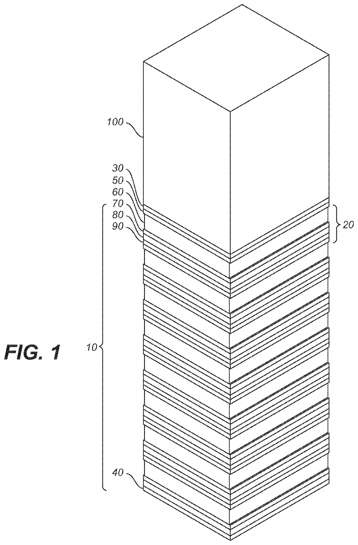
[0020]FIGS. 1-24 illustrate forming the active stacks of an HNOR memory array in two etching steps, according to the present invention. As shown in FIG. 1, memory structure 10 includes eight successively deposited active layers (e.g., active layer 20) of different materials between hard mask layer 30 and etch-stop layer 40. (Although FIG. 1 shows eight active layers, that number of active layers are provided merely for illustrative purpose only. Any suitable number of active layers may be provided, such as one, two, four, six, sixteen, thirty-two, or more active layers. Each active layer (e.g., active layer 20) may include: (i) first semiconductor layer (“source layer”) 50, (ii) first sacrificial layer (“SAC1”) layer 60, (iii) second semiconductor layer (“drain layer”) 70, (iv) second sacrificial layer (“SAC4”) 80 and (v) interlayer dielectric layer (“ILD layer”) 90. Source layer 50 and drain layer 70 may include any suitable semiconductor material (e.g., silicon, silicon germanium,...

second embodiment

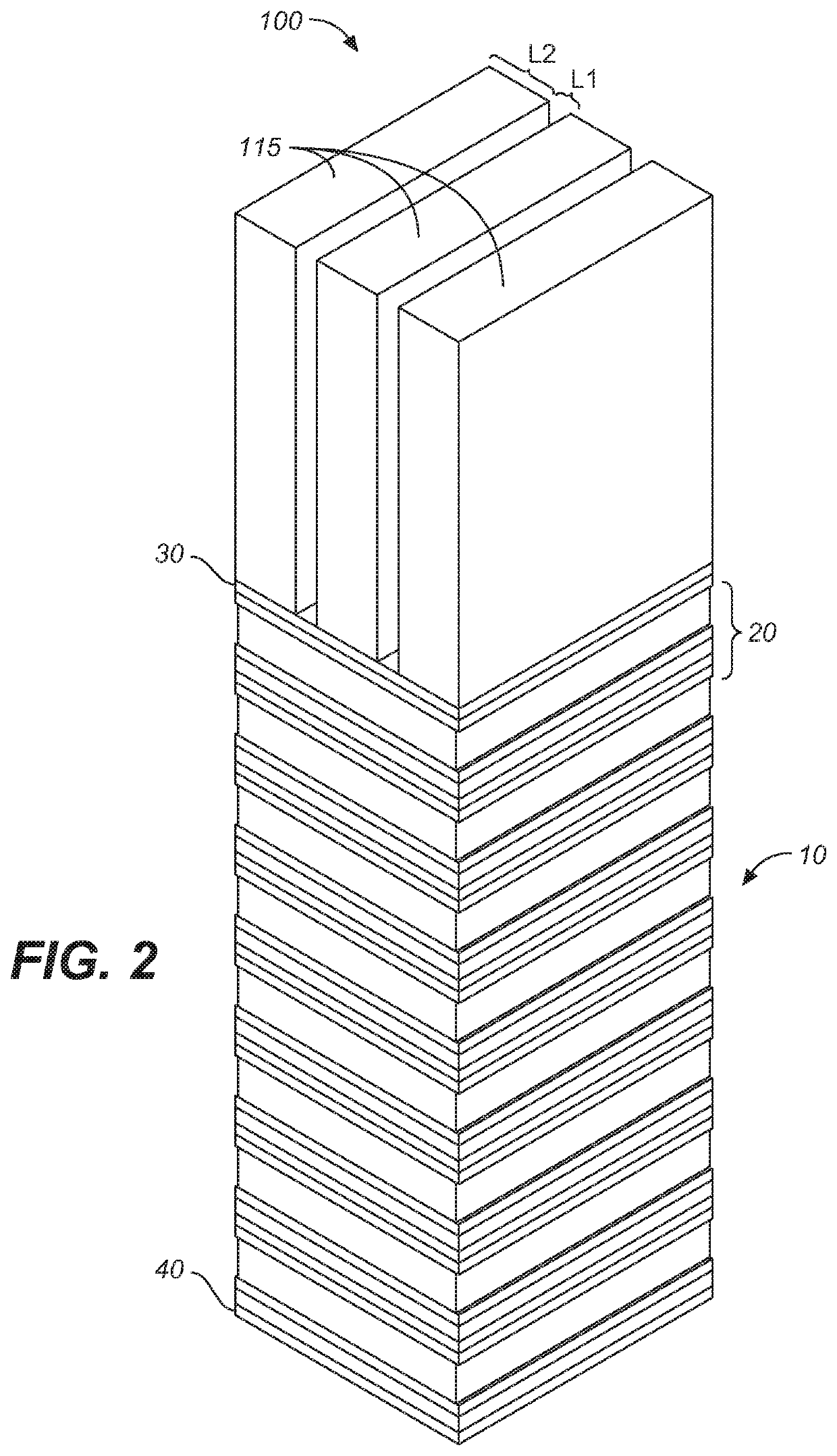
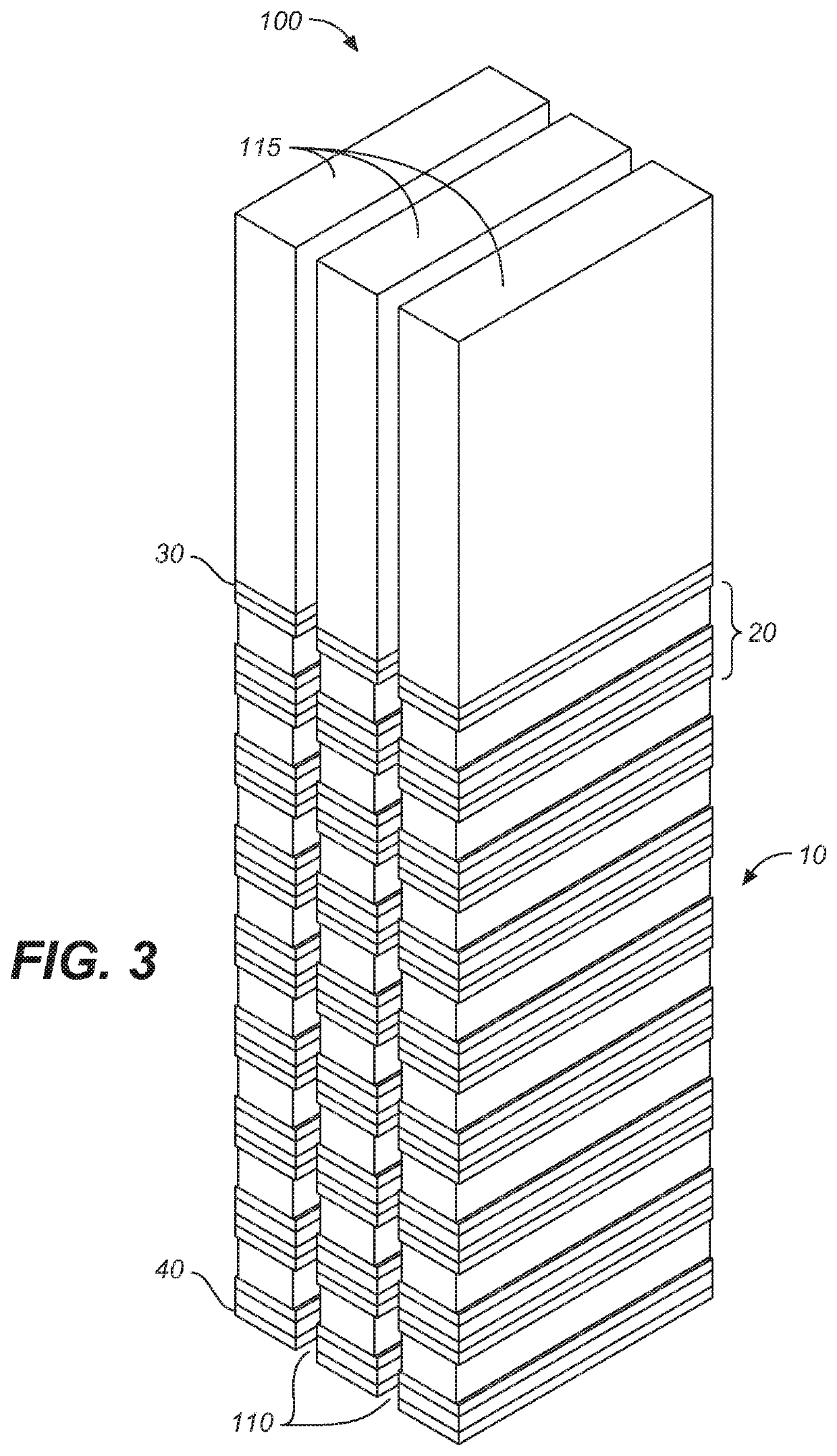
[0038]According to the present invention, as illustrated in FIGS. 25-36, a single etching step is used to etch the active layers into the active stacks of a HNOR memory array to avoid misalignment. To provide mechanical support, dielectric pillars are formed prior to etching the active layers to create the active stacks. These pillars lend support to the subsequently formed active stacks by maintaining their structural stability. Suitable choice of feature aspect ratios avoids ribboning during the high aspect ratio etch steps.

[0039]FIG. 25 shows memory structure 10 including eight active layers (e.g., active layer 20) between hard mask layer 30 and etch-stop layer 40, as in FIG. 1. The constituent layers of each active layer may be the same as those active layers discussed in conjunction with FIG. 1. Masking structure 500 allows memory structure 10 to be patterned and etched to etch-stop layer 40 to provide a set of vias 505 (not shown). After masking structure 500 is removed, vias ...

third embodiment

[0052]In an HNOR memory array according to the present invention, a typical nominal minimum width L1 of an active strip is 50 nanometers, while the nominal minimum width of trench 110 (FIG. 3) separating adjacent active stacks may be 80 nanometers, and the height of an active stack with eight active layers may be approximately 2,000 nanometers (2 microns). The aspect ratio of a stand-alone active stack of 50 nanometer width would therefore be 2000 / 50, or 40:1, which would be severely challenging to remain standing erect during an etch, let alone through successive process steps which would adversely impact yields and cost. However, using a method according to the first or the present invention, the width L2 of each masking structure 115 of FIG. 3 is 50+80+50=180 nanometers, therefore the aspect ratio of an etch using masking structures 115 is 2,000 / 180, or 11:1.

[0053]With a method according to the second embodiment, the active stacks are formed in one etch step, thereby avoiding the...


PUM

PropertyMeasurementUnit
aspect ratioaaaaaaaaaa
widthaaaaaaaaaa

Abstract

Various methods overcome the limitations and achieve superior scaling by (i) replacing a single highly challenging high aspect ratio etch step with two or more etch steps of less challenging aspect ratios and which involve wider and more mechanically stable active strips, (ii) using dielectric pillars for support and to maintain structural stability during a high aspect ratio etch step and subsequent processing steps, or (iii) using multiple masking steps to provide two or more etch steps of less challenging aspect ratios and which involve wider and more mechanically stable active strips.

Description

CROSS-REFERENCE TO RELATED APPLICATIONS[0001]The present application relates to and claims priority of (i) U.S. provisional application (“Provisional application I”), Ser. No. 62 / 775,310, entitled “Methods for Forming Multilayer Horizontal NOR-type Thin-film Memory Strings,” filed Dec. 4, 2018.[0002]The present invention also relates to (i) U.S. provisional application (“Provisional application II”), Ser. No. 62 / 697,085, entitled “Fabrication Method for a 3-Dimensional NOR Memory Array,” filed Jul. 12, 2018; (ii) U.S. provisional application (“Provisional application III”), Ser. No. 62 / 752,092, entitled “3-Dimensional NOR Memory Array with Very Fine Pitch: Device and Method,” filed on Oct. 29, 2018; and (iii) U.S. provisional patent application (“Provisional application IV”), Ser. No. 62 / 771,922, entitled “Staircase Structures for Electrically Connecting Multiple Horizontal Conductive Layers of a 3-Dimensional Memory Device,” filed on Nov. 27, 2018.[0003]The present application is a...

Claims


Application Information

Patent Timeline
Patent Type & Authority Applications(United States)
IPC IPC(8): H01L27/11582H01L21/308H01L29/66
CPCH01L27/11582H01L29/66833H01L21/308H10B41/50H10B43/50H10B41/27H10B43/27H10B41/20H10B43/20
Inventor HERNER, SCOTT BRADCHIEN, WU-YI HENRYZHOU, JIEHARARI, ELI
Owner SUNRISE MEMORY CORP
Why Eureka
Try Eureka