Semiconductor device

a technology of semiconductor devices and short-circuit capability, which is applied in the direction of semiconductor devices, basic electric elements, electrical equipment, etc., can solve the problems of insufficient short-circuit capability, taken in conventional technology, etc., and achieve the effect of improving short-circuit capability in semiconductor devices

Active Publication Date: 2020-06-18
MITSUBISHI ELECTRIC CORP
View PDF0 Cites 1 Cited by
  • Summary
  • Abstract
  • Description
  • Claims
  • Application Information

AI Technical Summary

Benefits of technology

[0006]According to the technology disclosed in the present application, the saturation current can be suppressed to improve the short-circuit capability.

Problems solved by technology

As described above, measures to suppress the saturation current to thereby improve the short-circuit capability have been taken in conventional technology, but have not yet been sufficient.

Method used


Image

  • Semiconductor device
  • Semiconductor device
  • Semiconductor device

Examples


first embodiment

[0025]A semiconductor device according to the present embodiment will be described below.

[0026]

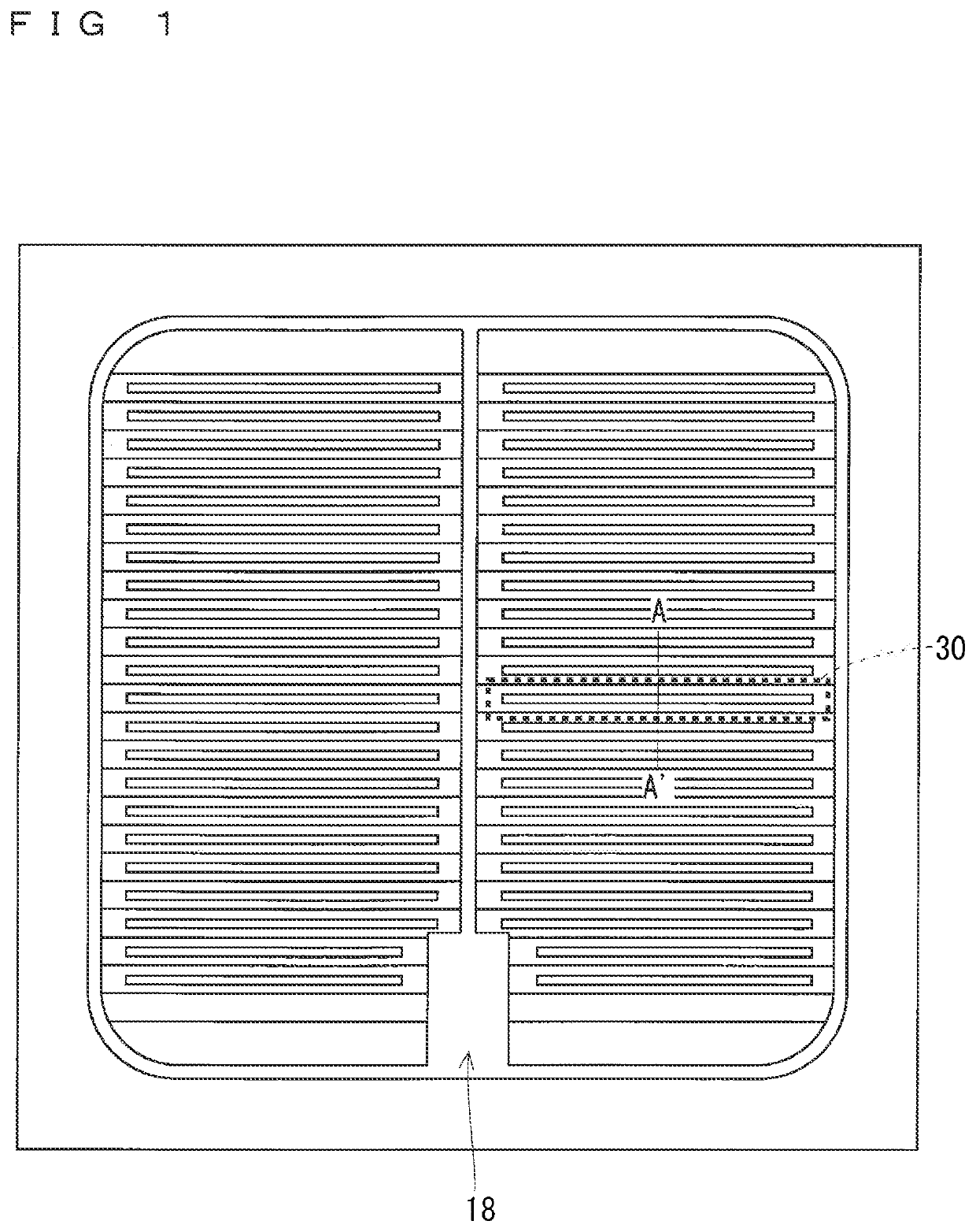
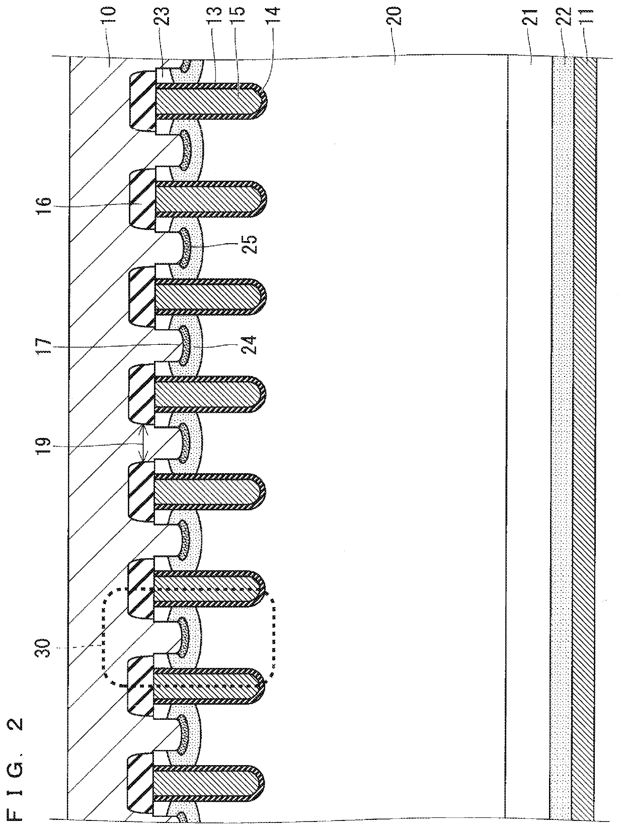
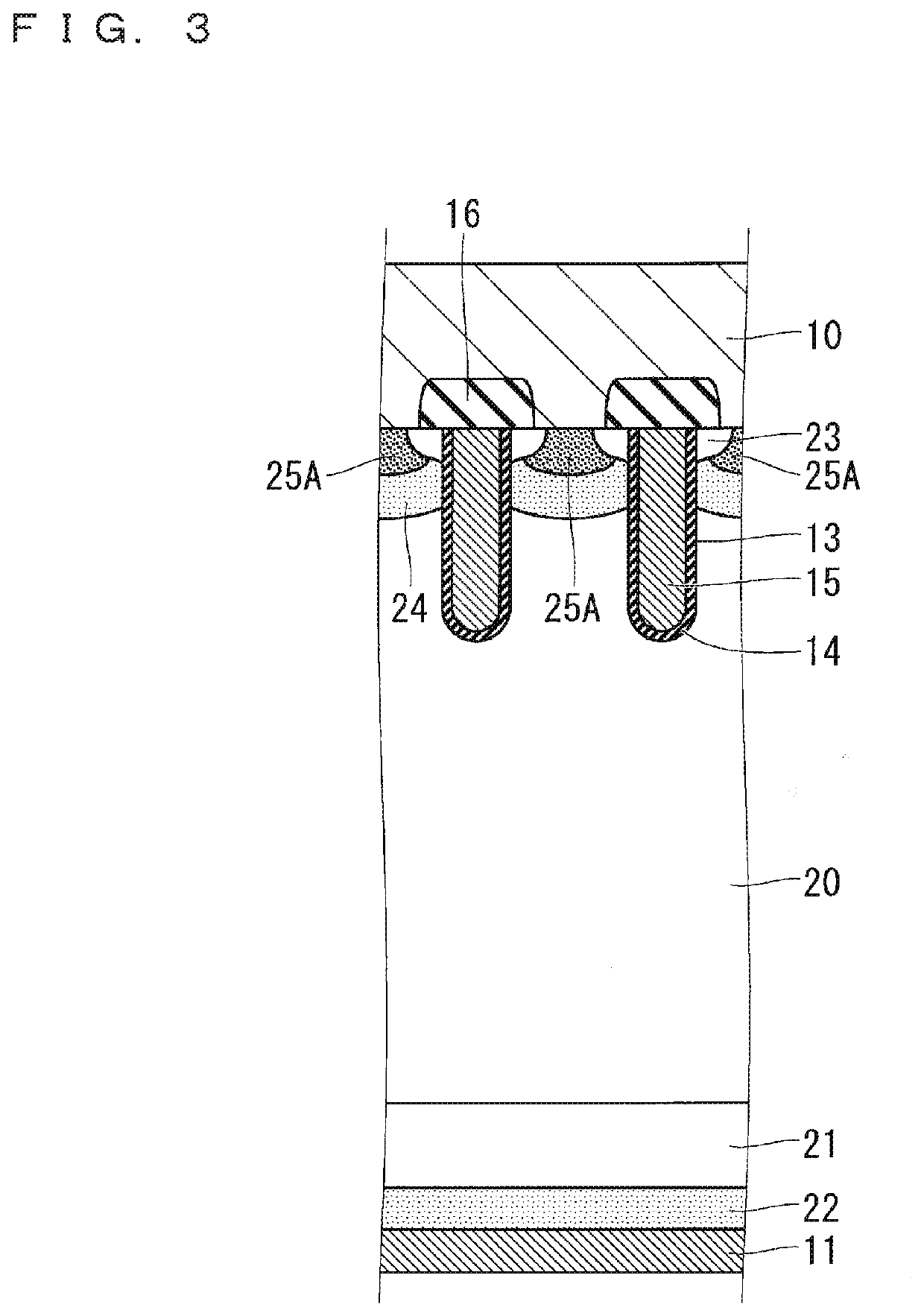
[0027]FIG. 1 is a plan view schematically showing an example of a configuration of the semiconductor device according to the present embodiment. FIG. 2 is a sectional view taken along a line A-A′ of FIG. 1.

[0028]As illustrated in FIG. 1, the semiconductor device includes an array of a plurality of cell regions 30 and a gate pad 18 disposed at the periphery of the array of the cell regions 30. Configurations of the cell regions 30 will be described below.

[0029]As illustrated in FIG. 2, the semiconductor device includes an n-type semiconductor substrate 20. The n-type semiconductor substrate 20 is made of Si, and has a first main surface (an upper surface in FIG. 2) and a second main surface (a lower surface in FIG. 2) opposing each other.

[0030]A p-type semiconductor layer 24 (a base layer) is formed in a surface layer on a side of the upper surface of the n-type semiconductor substrate 20. ...

second embodiment

[0079]A semiconductor device according to the present embodiment will be described below. In description made below, similar components to those described in the above-mentioned embodiment bear the same reference signs as those in the above-mentioned embodiment, and detailed description thereof is omitted as appropriate.

[0080]

[0081]FIG. 8 is a sectional view schematically showing an example of a configuration of the semiconductor device according to the present embodiment. FIG. 8 corresponds to a sectional view taken along the line A-A′ of FIG. 1.

[0082]As illustrated in FIG. 8, the semiconductor device in FIG. 8 includes the n-type semiconductor substrate 20, the p-type semiconductor layer 24, the n+-type semiconductor layer 23, the trenches 13, the gate dielectrics 14, the gate electrodes 15, the interlayer dielectrics 16, the contact trenches 17, the p+-type semiconductor layer 25, the emitter electrode 10, the n+-type buffer layer 21, the p-type collector layer 22, the collector ...


PUM

PropertyMeasurementUnit
widthaaaaaaaaaa
depthaaaaaaaaaa
depthaaaaaaaaaa

Abstract

A semiconductor device includes: a second semiconductor layer in a surface layer of a first semiconductor layer; a third semiconductor layer in a surface layer of the second semiconductor layer; a first trench penetrating the second semiconductor layer and the third semiconductor layer to reach an inside of the first semiconductor layer; a second trench penetrating, from an upper surface of the first semiconductor layer, the third semiconductor layer to reach an inside of the second semiconductor layer, and a fourth semiconductor layer in contact with a bottom of the second trench.

Description

BACKGROUND OF THE INVENTIONField of the Invention[0001]Technology disclosed in the present application relates to semiconductor devices.Description of the Background Art[0002]In an insulated gate bipolar transistor (IGBT) having a trench gate structure as exemplified in Japanese Patent Application Laid-Open No. 2001-250947, for example, a method of increasing a threshold voltage has typically been taken to suppress a saturation current to thereby improve short-circuit capability.[0003]As described above, measures to suppress the saturation current to thereby improve the short-circuit capability have been taken in conventional technology, but have not yet been sufficient.SUMMARY[0004]It is an object of technology disclosed in the present application to provide technology for suppressing a saturation current to improve short-circuit capability in a semiconductor device.[0005]The technology disclosed in the present application includes: a first semiconductor layer of a first conductivi...

Claims


Application Information

Patent Timeline
Patent Type & Authority Applications(United States)
IPC IPC(8): H01L29/739
CPCH01L29/7397H01L27/0823H01L29/0684H01L29/423H01L29/7396H01L29/1095H01L29/0619H01L29/0696H01L2224/0603
Inventor HARADA, TATSUO
Owner MITSUBISHI ELECTRIC CORP
Why Eureka
Try Eureka