Display Device

a display device and display technology, applied in the field of display devices, can solve the problem of limit in maximizing the display area of the display device, and achieve the effect of reducing the non-display area and preventing damage to the light emitting stack

Active Publication Date: 2020-06-18
LG DISPLAY CO LTD
View PDF0 Cites 26 Cited by
  • Summary
  • Abstract
  • Description
  • Claims
  • Application Information

AI Technical Summary

Benefits of technology

[0007]An object of the present invention is to provide a display device capable of reducing a non-display area.
[0009]To achieve these objects and other advantages and in accordance with the purpose of the disclosure, as embodied and broadly described herein, a display device includes a substrate hole surrounded by light emitting elements, and a moisture penetration preventing layer disposed between an inner dam surrounded by the light emitting elements and the substrate hole. Accordingly, it may be possible to prevent damage to light emitting stacks caused by external moisture or oxygen. Since the substrate hole is disposed within an active area, a reduction in non-display area may be achieved.

Problems solved by technology

For this reason, there may be a limitation in maximizing a display area in the display device.

Method used


Image

  • Display Device
  • Display Device
  • Display Device

Examples


first embodiment

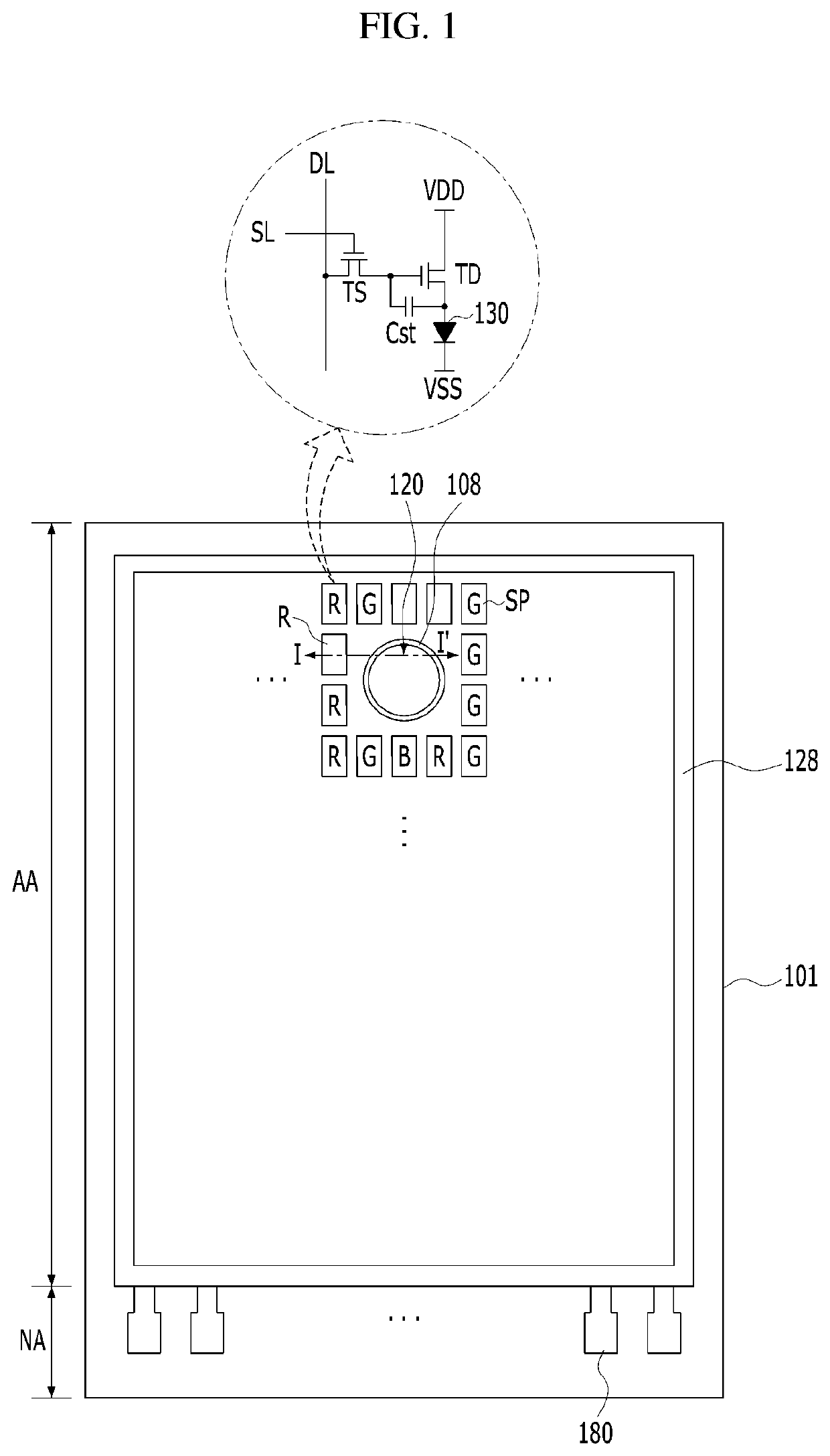
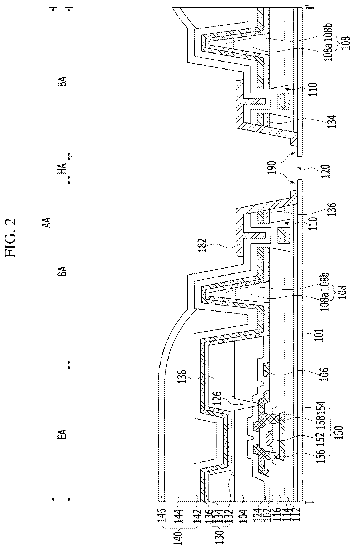
[0032]FIG. 2 illustrates an organic light emitting display device according to the present disclosure. As illustrated in FIG. 2, the driving transistor TD, which is designated by reference numeral “150”, includes an active layer 154 disposed on an active buffer layer 114, a gate electrode 152 overlapping with the active layer 154 under the condition that a gate insulating film 116 is interposed between the active layer 154 and the gate electrode 152, and source and drain electrodes 156 and 158 formed on an interlayer insulating film 102 while contacting the active layer 154.

[0033]The active layer 154 is made of at least one of an amorphous semiconductor material, a polycrystalline semiconductor material or an oxide semiconductor material. The active layer 154 includes a channel region, a source region and a drain region. The channel region overlaps with the gate electrode 152 under the condition that the gate insulating film 116 is interposed between the channel region and the gate ...

second embodiment

[0060]FIG. 5 is a cross-sectional view illustrating an organic light emitting display device according to the present disclosure.

[0061]The organic light emitting display device illustrated in FIG. 5 includes the same constituent elements as those of the organic light emitting display device illustrated in FIG. 2, except that a black layer 184 is further included. Accordingly, no detailed description will be given of the same constituent elements for the sake of brevity.

[0062]The black layer 184 is formed over the moisture penetration preventing layer 182 such that the black layer 184 has a greater width than the moisture penetration preventing layer 182. That is, the black layer 184 is formed to cover upper and side surfaces of the moisture penetration preventing layer 182 disposed in the barrier area BA such that the black layer 184 contacts the upper and side surfaces of the moisture penetration preventing layer 182. Accordingly, it may be possible to prevent externally incident l...

third embodiment

[0065]FIG. 7 is a cross-sectional view illustrating a display device including a substrate hole according to the present disclosure.

[0066]The display device illustrated in FIG. 7 includes the same constituent elements as those of the display device illustrated in FIG. 2, except that a touch sensor is further included. Accordingly, no detailed description will be given of the same constituent elements for the sake of brevity.

[0067]The touch sensor includes a plurality of touch electrodes 192, and a plurality of bridges 194 connecting the touch electrodes 192.

[0068]At least one of each touch electrode 192 or each bridge 194 may be constituted by a transparent conductive film made of ITO or IZO, may be constituted by a mesh metal film having a mesh structure, or may be constituted by a transparent conductive film as described above and a mesh metal film disposed over or beneath the transparent conductive film. Here, the mesh metal film is formed to have a mesh structure, using at least...


PUM

PropertyMeasurementUnit
areaaaaaaaaaaa
active areaaaaaaaaaaa
non-active areaaaaaaaaaaa

Abstract

A display device capable of reducing a non-display area includes a substrate hole surrounded by light emitting elements, and a moisture penetration preventing layer disposed between an inner dam surrounded by the light emitting elements and the substrate hole. Accordingly, it is possible to prevent damage to light emitting stacks caused by external moisture or oxygen. Since the substrate hole is disposed within an active area, a reduction in non-display area is achieved.

Description

CROSS-REFERENCE TO RELATED APPLICATIONS[0001]This application claims the benefit of Republic of Korea Patent Application No. 10-2018-0161834 filed on Dec. 14, 2018, which is hereby incorporated by reference as if fully set forth herein.BACKGROUNDField[0002]The present disclosure relates to a display device, and more particularly to a display device capable of reducing a non-display area.Discussion of the Related Art[0003]An image display device, which renders a variety of information on a screen, is a core technology of the information age. Such an image display device is developing towards enhanced thinness, enhanced lightness, and enhanced portability as well as enhanced performance. In connection with this, a flat display device capable of eliminating disadvantages of heavy and bulky structures of cathode ray tubes (CRTs) is highlighted.[0004]Representative examples of such a flat display device may include a liquid crystal display (LCD) device, a plasma display panel (PDP), an o...

Claims


Application Information

Patent Timeline
Patent Type & Authority Applications(United States)
IPC IPC(8): H01L51/52H01L27/32G06F3/041G06F3/042
CPCH01L51/5253H01L51/5284H01L27/3246G06F3/0412H01L27/3234H01L27/323H01L51/5246G06F2203/04107G06F3/0425H10K59/32H10K59/88H10K59/00H10K59/12G06F2203/04103H10K50/844H10K59/351H10K59/40H10K50/846H10K50/865H10K50/8426H10K59/65H10K59/122
Inventor LEE, YOUNG-WOOKHWANG, SEON-HUIPARK, EUN-YOUNGAN, YONG-SUCHO, WOO-CHANLEE, SUN-MIPARK, JONG-HAN
Owner LG DISPLAY CO LTD
Why Eureka
Try Eureka