

Organic electroluminescence device, method for manufacturing organic electroluminescence device, and electronic apparatus
- Summary
- Abstract
- Description
- Claims
- Application Information
AI Technical Summary
Benefits of technology
Problems solved by technology
Method used
Image

Examples
first embodiment
1-1. First Embodiment
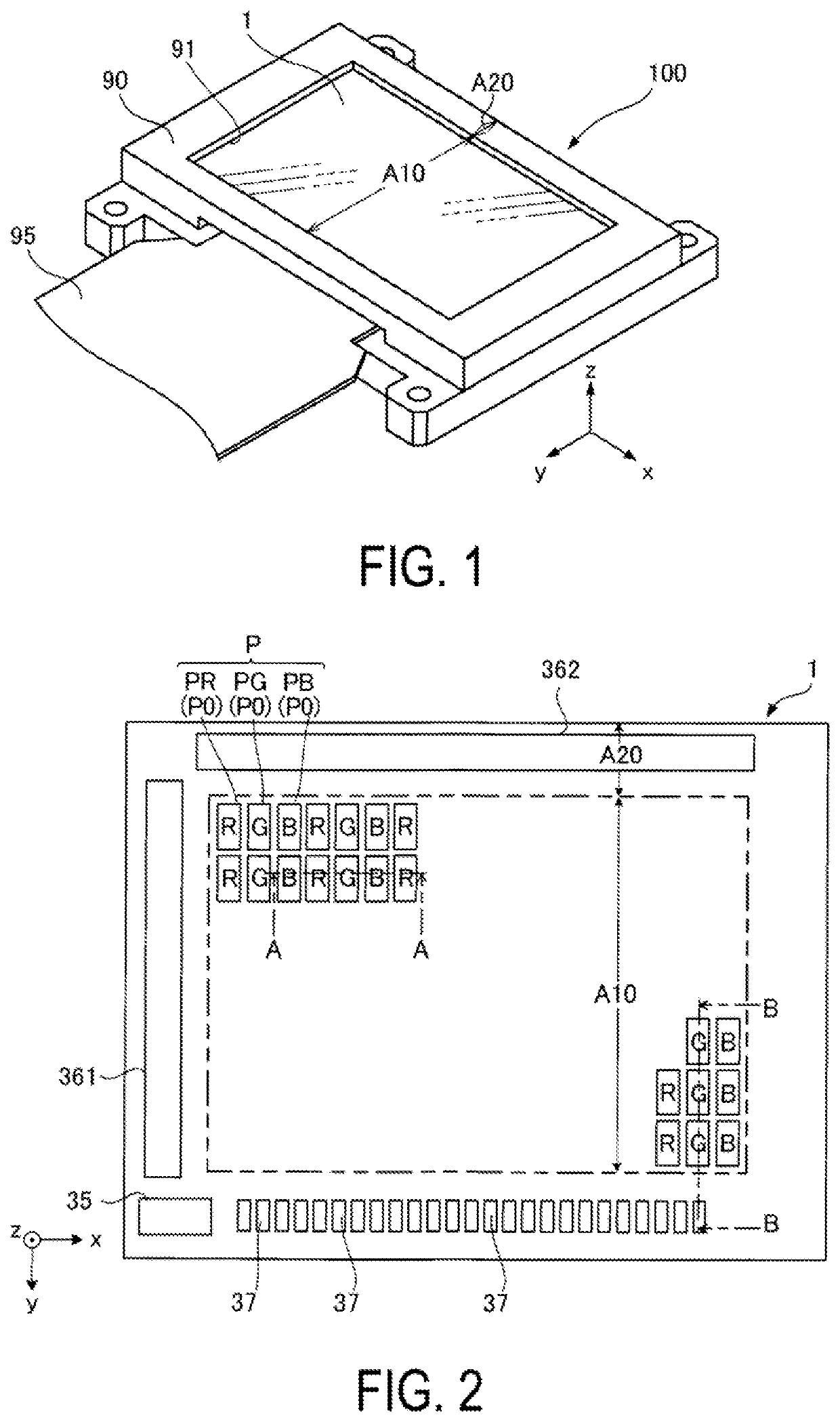
[0033]FIG. 1 is a perspective view illustrating a configuration of an organic EL device 100 according to a first embodiment. Note that, for convenience of explanation, the description will be made appropriately using an x-axis, a y-axis, and a z-axis orthogonal to each other illustrated in FIG. 1. A surface of a transmissive substrate 7 included in a display panel 1 described later is parallel to an x-y plane, and a lamination direction of a plurality of layers included in the display panel 1 described later is a z direction.
[0034]1-1A. Overall Configuration of Organic EL Device 100
[0035]The organic EL device 100 illustrated in FIG. 1 is an example of an “organic electroluminescence device”, and is an organic EL display device configured to display a full color image. The organic EL device 100 is used as a micro display configured to display an image in a head-mounted display, for example. Note that the head-mounted display will be described later in detail.
[003...
second embodiment
1-2. Second Embodiment
[0133]FIG. 20 is a partial cross-sectional view of a display panel 1A according to a second embodiment. The present embodiment is different from the first embodiment in that the present embodiment includes a third protecting portion 65. Note that, in the second embodiment, a sign used in the description of the first embodiment is used for the same matter as that of the first embodiment, and each detailed description thereof will be appropriately omitted.
[0134]A color filter layer 6A of the display panel 1A illustrated in FIG. 20 covers a protecting portion 4. The color filter layer 6A is in contact with an outer circumferential surface 420 of a second layer 42. Furthermore, the color filter layer 6A is in contact with an outer circumferential surface 410 of a first layer 41 and an outer circumferential surface 430 of a third layer 43. In other words, in the present embodiment, the color filter layer 6A is in contact with an outer circumferential surface 40 of t...
third embodiment
1-3. Third Embodiment
[0138]FIG. 21 is a partial cross-sectional view of a display panel 1B according to a third embodiment. FIG. 22 is a plan view of the display panel 1B according to the third embodiment. The present embodiment is mainly different from the first embodiment in that a protecting portion 4B includes an opening 49. Note that, in the second embodiment, a sign used in the description of the first embodiment is used for the same matter as that of the first embodiment, and each detailed description thereof will be appropriately omitted. Further, a transmissive substrate 7 is not illustrated in FIG. 22. Further, in FIG. 22, shading is provided to an adhesive layer 70B in order to facilitate understanding of the arrangement of the adhesive layer 70B.
[0139]As illustrated in FIGS. 21 and 22, the opening 49 that overlaps a plurality of terminals 37 in plan view is provided in the protecting portion 4B of the display panel 1B. The opening 49 is a space that penetrates the protec...
PUM
 Abstract
Description
Claims
Application Information