Light emitting display device and method for manufacturing the same

a technology of light-emitting display and manufacturing method, which is applied in the direction of semiconductor devices, semiconductor/solid-state device details, electrical apparatus, etc., can solve problems such as color change, and achieve the effect of reducing the thickness of the first portion

Active Publication Date: 2020-07-30
SAMSUNG DISPLAY CO LTD
View PDF0 Cites 0 Cited by
  • Summary
  • Abstract
  • Description
  • Claims
  • Application Information

AI Technical Summary

Benefits of technology

The patent describes a display screen that produces light on its own. The design of the screen can cause color distortion when the viewer's perspective changes. The technical effect of this design is to improve the color accuracy of the display screen.

Problems solved by technology

This may cause a color change when a viewing angle changes.

Method used


Image

  • Light emitting display device and method for manufacturing the same
  • Light emitting display device and method for manufacturing the same
  • Light emitting display device and method for manufacturing the same

Examples


Embodiment Construction

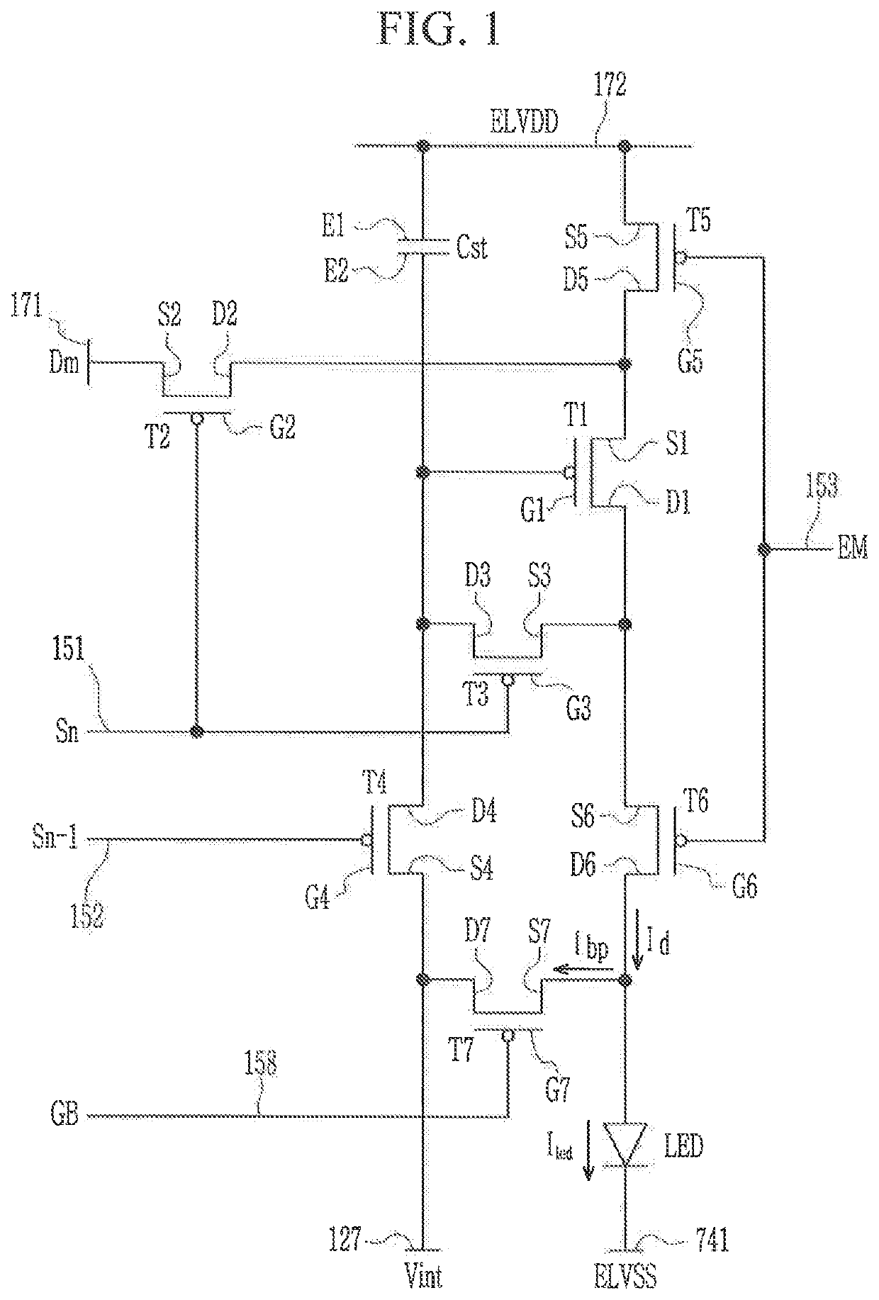
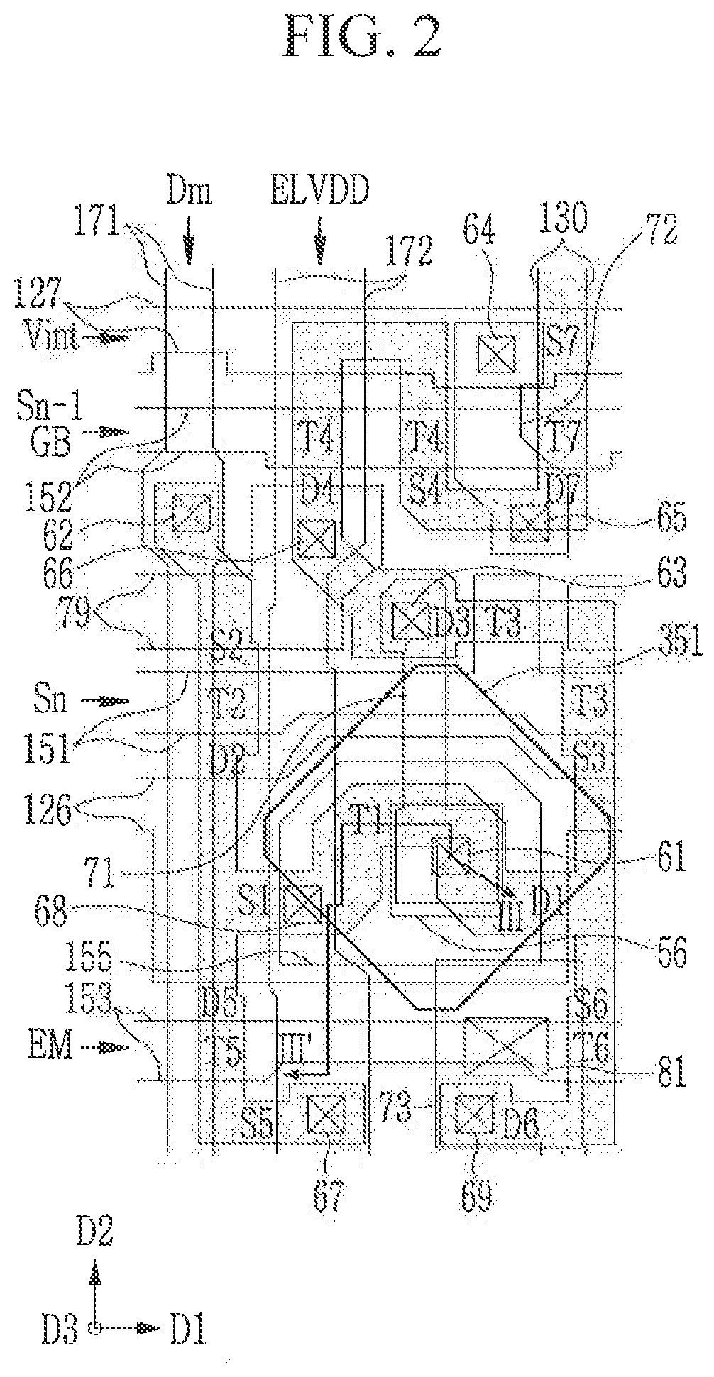
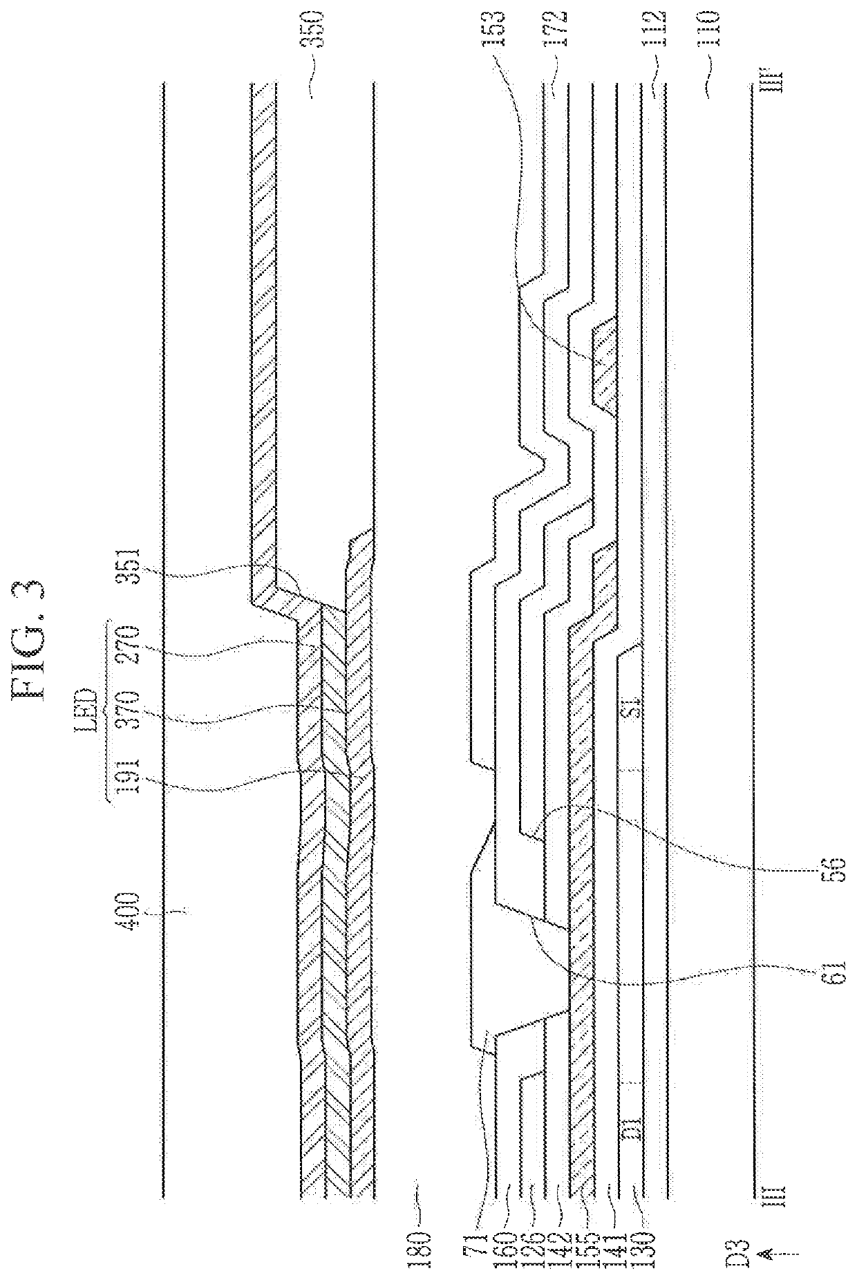
[0035]Exemplary embodiments of the present invention will be described more fully hereinafter with reference to the accompanying drawings. As those skilled in the art would realize, the described exemplary embodiments may be modified in various different ways, and thus should not be limited to the embodiments set forth herein.

[0036]In the figures, like reference numerals may denote like elements or features, and thus their descriptions may be omitted.

[0037]Further, in the drawings, the size and thickness of each element may be exaggerated for clarity.

[0038]It will be understood that when an element such as a layer, film, region, or substrate is referred to as being “on” another element, it can be directly on the other element or intervening elements may also be present.

[0039]Further, throughout the specification, the phrase “on a plane” may mean viewing a target portion from the top, and the phrase “on a cross-section” may mean viewing a cross-section formed by vertically cutting a ...


PUM

PropertyMeasurementUnit
areaaaaaaaaaaa
photosensitiveaaaaaaaaaa
thicknessaaaaaaaaaa

Abstract

A light emitting display device includes: a substrate; a semiconductor layer disposed on the substrate; a first insulating layer disposed on the semiconductor layer; a first gate conductor disposed on the first insulating layer; a second insulating layer disposed on the first gate conductor; a second gate conductor disposed on the second insulating layer; an interlayer insulating layer disposed on the second gate conductor; a data conductor disposed on the interlayer insulating layer; a passivation layer disposed on the data conductor; a diode first electrode disposed on the passivation layer; a partition wall disposed on the diode first electrode and including an opening overlapping the diode first electrode; a light emitting layer; and a diode second electrode. The data conductor includes a first inclined surface and a second inclined surface, and an area of the first inclined surface is different from an area of the second inclined surface.

Description

CROSS-REFERENCE TO RELATED APPLICATION[0001]This application claims priority under 35 § 119 to Korean Patent Application Na 10-2019-0009439 filed in the Korean Intellectual Property Office on Jan. 24, 2019, the disclosure of which is incorporated by reference herein in its entirety.TECHNICAL FIELD[0002]The present invention relates to a light emitting display device and a method for manufacturing the same.DISCUSSION OF RELATED ART[0003]In general, when a light emitting display device has a self-emission characteristic, it does not use an additional light source. Therefore, it is possible to reduce thickness and weight of a self-emissive display device. Further, the self-emissive light emitting display device may have additional qualities such as low power consumption, high luminance, and high response speed.[0004]The self-emissive light emitting display device may include a light emitting diode including two electrodes and a light emitting layer disposed between the two electrodes. ...

Claims


Application Information

Patent Timeline
Patent Type & Authority Applications(United States)
IPC IPC(8): H01L27/32
CPCH01L27/3297H01L27/326H01L27/156H01L27/124H01L27/0203H01L23/50H10K59/80521H10K59/80515H10K59/122H10K59/131H01L27/1214H01L33/38H01L33/62H01L33/005H01L21/0274H10K59/121
Inventor HONG, SANG MINJEONG, HEE SEONG
Owner SAMSUNG DISPLAY CO LTD
Why Eureka
Try Eureka