Integrated circuit package having pin up interconnect

a technology of integrated circuits and interconnects, which is applied in the manufacture of printed circuits, basic electric elements, solid-state devices, etc., can solve the problems of reducing the thickness of the first patterned conductive layer, causing defects, and affecting the quality of the printed substra

Active Publication Date: 2017-11-09
QDOS FLEXCIRCUITS
View PDF5 Cites 0 Cited by
  • Summary
  • Abstract
  • Description
  • Claims
  • Application Information

AI Technical Summary

Benefits of technology

The invention describes a method for making a conductive layer by creating a pattern on a surface and then removing excess material using a process called trimming. The result is a layer with a reduced thickness, making it suitable for use in various applications. This technique helps to improve the efficiency and reliability of the process for making conductive layers.

Problems solved by technology

However, the glass epoxy print substrate may cause a problem that the heat treatments performed in fabrication of the build-up multi-layered substrate may bring the glass epoxy print substrate to a poor condition and creating defects.
Furthermore, the heat treatments carried out at the time of chip loading and solder reflow may cause the faulty connection and the distortion which affects the long-term reliability for the connection.
Moreover, the interconnecting substrate for packaging is mounted on an external board or apparatus, the stress is structurally centered on the interface between the external electrode terminal and the insulating layer, which tends to give rise to opening defects so that the satisfactory mounting reliability cannot be obtained.

Method used


Image

  • Integrated circuit package having pin up interconnect
  • Integrated circuit package having pin up interconnect
  • Integrated circuit package having pin up interconnect

Examples


Embodiment Construction

[0093]To further clarify various aspects of some embodiments of the present invention, a more particular description of the invention will be rendered by references to specific embodiments thereof, which are illustrated in the appended drawings. It is appreciated that these drawings depict only typical embodiments of the invention and are therefore not to be considered limiting of its scope. The invention will be described and explained with additional specificity and detail through the accompanying drawings in which:

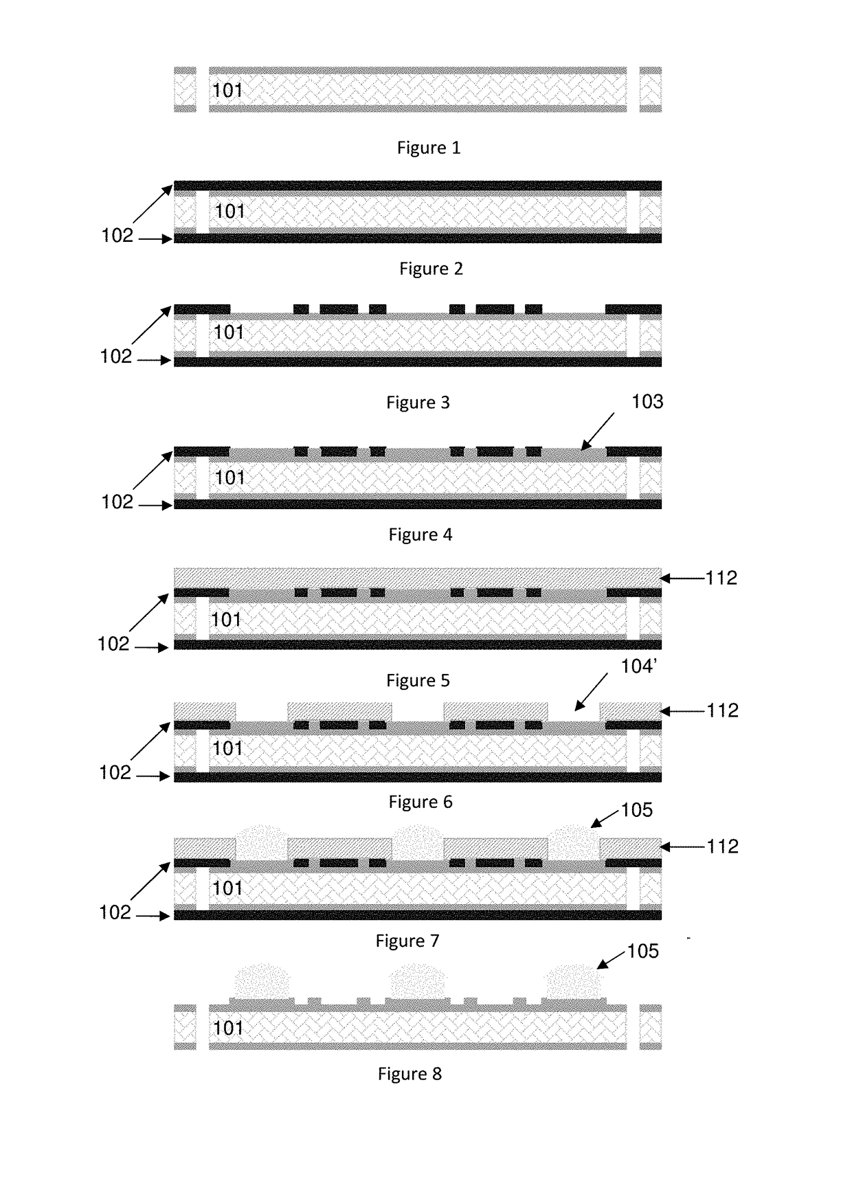
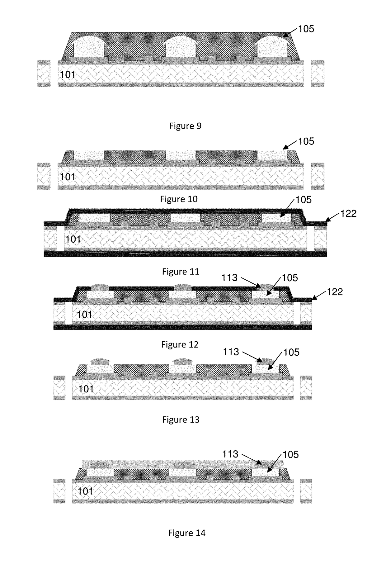
[0094]FIGS. 1-25 are detailed process flowcharts of manufacturing and connecting for an integrated circuit package according to a first embodiment of the invention.

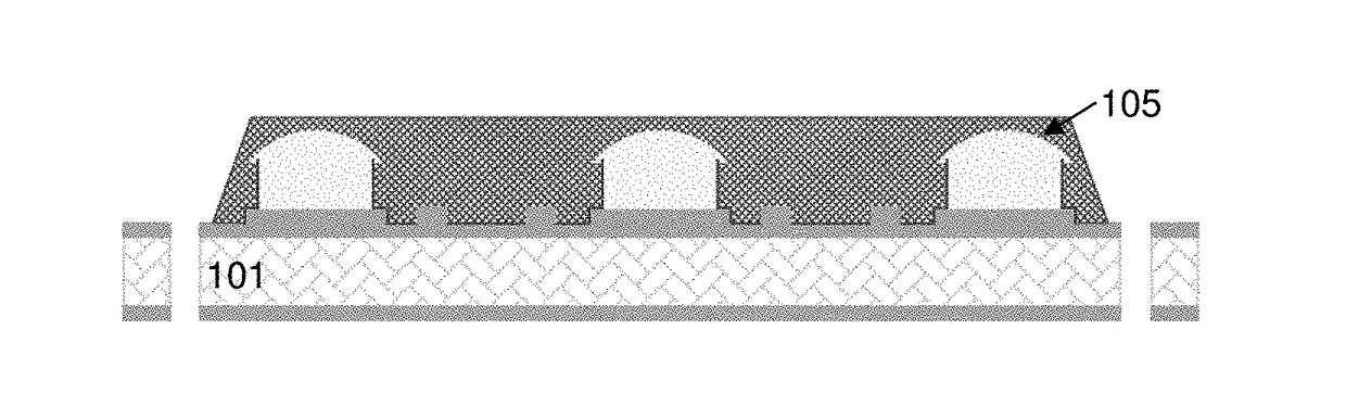
[0095]FIG. 1 illustrates an integrated circuit package according to at least one embodiment of the invention. Firstly, a carrier or base (101) is established or developed, wherein the base (101) is a steel material or copper or conductive material such as charge carrier. Preferably, the carbon steel or steel ...


PUM


Abstract

An integrated circuit package and manufacturing method thereof are described. The integrated circuit package includes pin up conductive plating to form an interconnect, where an opening on a patterned fifth layer photo-resist material located at bottom portion of a base developed for etching selectively the base to form at least an internal opening and at least a positioning opening, wherein the internal opening corresponds with an inside area of a first patterned conductive layer, and the positioning opening corresponds with an outside area of the first patterned conductive layer.

Description

CROSS-REFERENCE TO RELATED APPLICATION[0001]The instant application claims priority to Malaysia Patent Application Serial No. PI 2016701182 filed Mar. 31, 2016, the entire specification of which is expressly incorporated herein by reference.FIELD OF THE INVENTION[0002]The invention relates in general to an integrated circuit package and manufacturing method thereof, and more particularly to an integrated circuit package having pin up conductive plating to form an interconnect.BACKGROUND OF THE INVENTION[0003]Recently, there was an increase in the number of terminals and the narrowing of their pitches in the semiconductor or integrated circuit device which result from advancements in the performance of operations, the capability of performing multi tasks and the integration thereof, which results in the growing demands of the interconnecting substrate for packaging which carries the semiconductor device also attains a higher density in arrangement and interconnections.[0004]The curre...

Claims


Application Information

Patent Timeline
Patent Type & Authority Applications(United States)
IPC IPC(8): H01L21/82H01L23/498H01L21/311H01L21/762H01L23/522
CPCH01L21/82H01L23/49827H01L23/522H01L21/311H01L21/762H01L23/49811H01L23/12H01L23/49822H01L21/4857H01L21/486H01L23/538H01L23/4924H05K1/113H05K3/4007H05K3/4647H05K3/4038H05K3/4661H05K3/184H01L23/5226
Inventor LOW, LOKE CHEWYUAN, LINHUI
Owner QDOS FLEXCIRCUITS
Why Eureka
Try Eureka