Eureka AIR delivers breakthrough ideas for toughest innovation challenges, trusted by R&D personnel around the world.

Impedance matching network and method

Active Publication Date: 2020-10-29
RENO TECH
View PDF0 Cites 0 Cited by
  • Summary
  • Abstract
  • Description
  • Claims
  • Application Information

AI Technical Summary

Benefits of technology

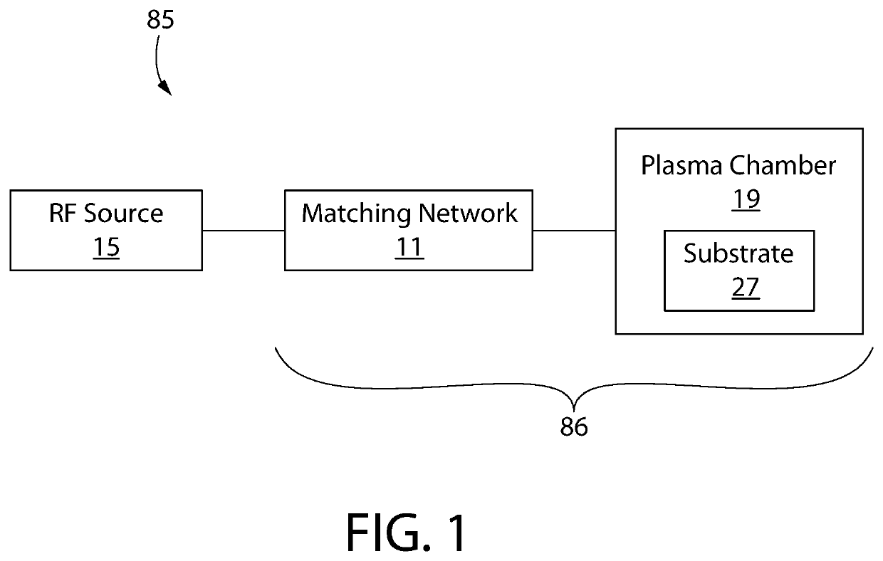
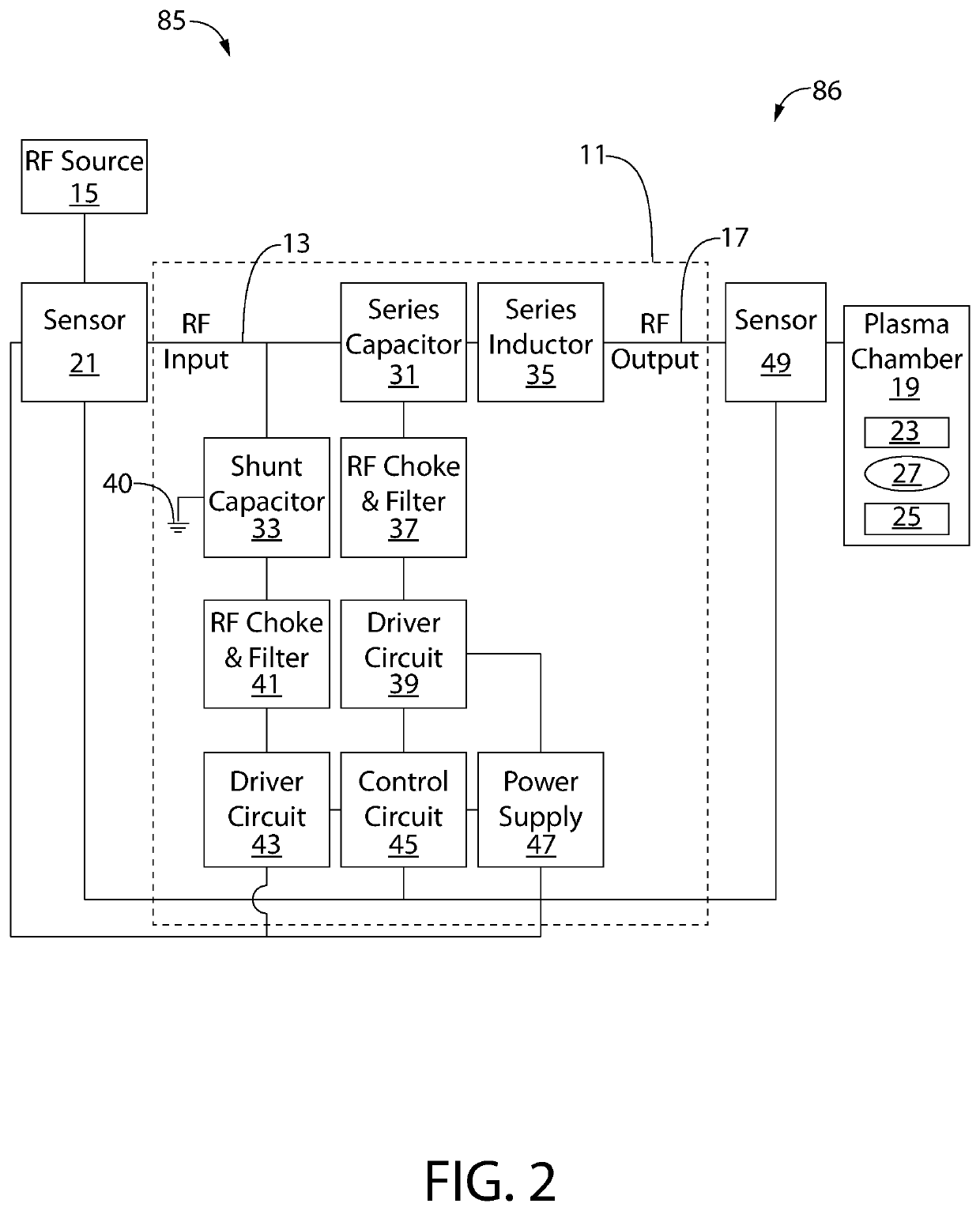
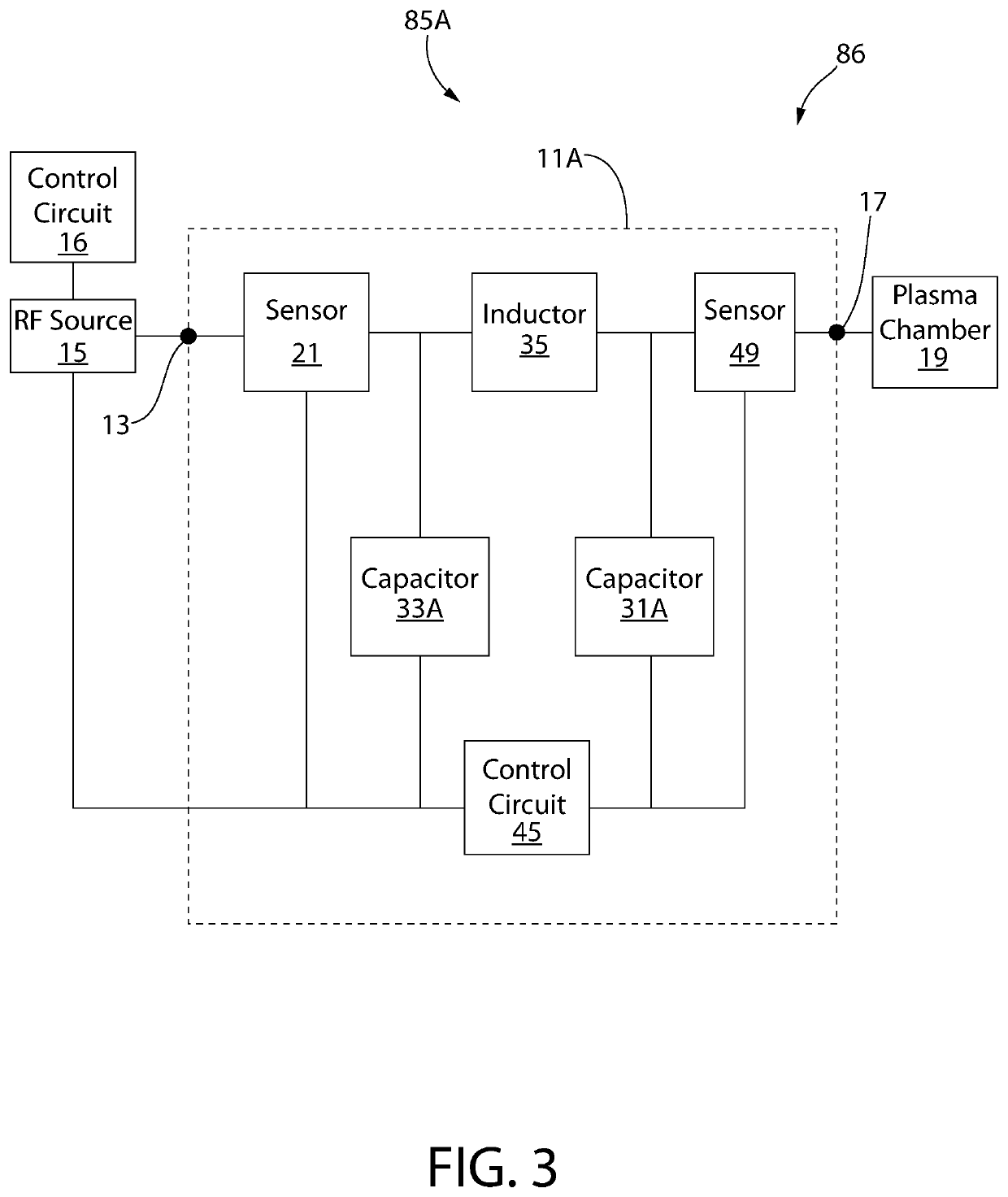
The present disclosure is about an impedance matching network used in a semiconductor processing tool. The network includes a variable capacitor and switches that can alter the capacitance of the network. The network is controlled by a control circuit that determines the optimal matching based on a measured parameter. The control circuit can adjust the capacitance of the network by a limited amount, based on a predetermined blocking voltage. This permits more efficient and accurate impedance matching, leading to improved performance of the semiconductor processing tool. The patent also describes a method of manufacturing a semiconductor device by using an impedance matching network during a plasma process. The process involves placing a substrate in a plasma chamber and coupling the impedance matching network between an RF source and the chamber for impedance matching. This leads to better quality materials deposition and etching, resulting in improved performance of semiconductor devices.

Problems solved by technology

In complex semiconductor processes, where the impedance changes are very rapid, the rapid and frequent movements put stresses on the VVC leading to their failures.
As semiconductor devices shrink in size and become more complex, however, the feature geometries become very small.
Current RF matching networks take 1-2 seconds to tune the process and this results in unstable process parameters for a significant portion of the process time.
While EVC technology is known, it has yet to be developed into an industry-accepted replacement for VVCs.
However, because an EVC is purely an electronic device, an EVC is not a one-for-one replacement for a VVC in an RF matching network.

Method used


Image

  • Impedance matching network and method
  • Impedance matching network and method
  • Impedance matching network and method

Examples


Embodiment Construction

[0034]The following description of the preferred embodiment(s) is merely exemplary in nature and is in no way intended to limit the invention or inventions. The description of illustrative embodiments is intended to be read in connection with the accompanying drawings, which are to be considered part of the entire written description. In the description of the exemplary embodiments disclosed herein, any reference to direction or orientation is merely intended for convenience of description and is not intended in any way to limit the scope of the present inventions. The discussion herein describes and illustrates some possible non-limiting combinations of features that may exist alone or in other combinations of features. Furthermore, as used herein, the term “or” is to be interpreted as a logical operator that results in true whenever one or more of its operands are true. Furthermore, as used herein, the phrase “based on” is to be interpreted as meaning “based at least in part on,” ...


PUM


Abstract

In one embodiment, the present disclosure may be directed to an impedance matching network that includes an electronically variable capacitor (EVC). The EVC includes discrete capacitors and corresponding switches, each switch configured to switch in and out one of the discrete capacitors to alter a capacitance of the EVC. The switches are operably coupled to a power supply providing a blocking voltage to the switches. A control circuit determines a blocking voltage value of the power supply. Upon determining the blocking voltage value is at or below a predetermined first level, the control circuit causes a limited altering of the capacitance of the EVC, the limited altering limiting the number or type of discrete capacitors to switch in or out based on the extent to which the blocking voltage value is at or below the first level.

Description

CROSS REFERENCE TO RELATED APPLICATIONS[0001]The present application is a continuation in part of U.S. patent application Ser. No. 16 / 839,424, filed Apr. 3, 2020, which is a continuation of U.S. patent application Ser. No. 16 / 804,324, filed Feb. 28, 2020, which is a continuation in part of U.S. patent application Ser. No. 16 / 685,698, filed Nov. 15, 2019, which is a continuation in part of U.S. patent application Ser. No. 16 / 592,453, filed Oct. 3, 2019, which is a continuation in part of U.S. patent application Ser. No. 16 / 524,805, filed Jul. 29, 2019, which is a continuation in part of U.S. patent application Ser. No. 16 / 502,656, filed Jul. 3, 2019, which is a continuation in part of U.S. patent application Ser. No. 16 / 029,742, filed Jul. 9, 2018, which claims the benefit of U.S. Provisional Patent Application No. 62 / 530,446, filed Jul. 10, 2017. U.S. patent application Ser. No. 16 / 502,656 further claims the benefit of U.S. Provisional Patent Application No. 62 / 693,625, filed Jul. 3...

Claims


Application Information

Patent Timeline
IPC IPC(8): H01J37/32H03H7/38H01L21/02H01L21/311H01L21/3213H01L21/285H01L21/67H03H7/40
CPCH01L21/28556H03H7/40H01L21/67069H03H7/38H01L21/31138H01J2237/334H01L21/31116H01L21/02274H01J37/32183H01J2237/332H01L21/32136
Inventor BHUTTA, IMRAN AHMEDDECKER, RONALD ANTHONYULRICH, MICHAEL GILLIAMKANDAMPALAYAM, BALA
Owner RENO TECH
Why Eureka
Eureka Blog
Learn More