

Binary-to-ternary converter using a complementary resistive switch
- Summary
- Abstract
- Description
- Claims
- Application Information
AI Technical Summary
Benefits of technology
Problems solved by technology
Method used
Image



Examples
first exemplary embodiment
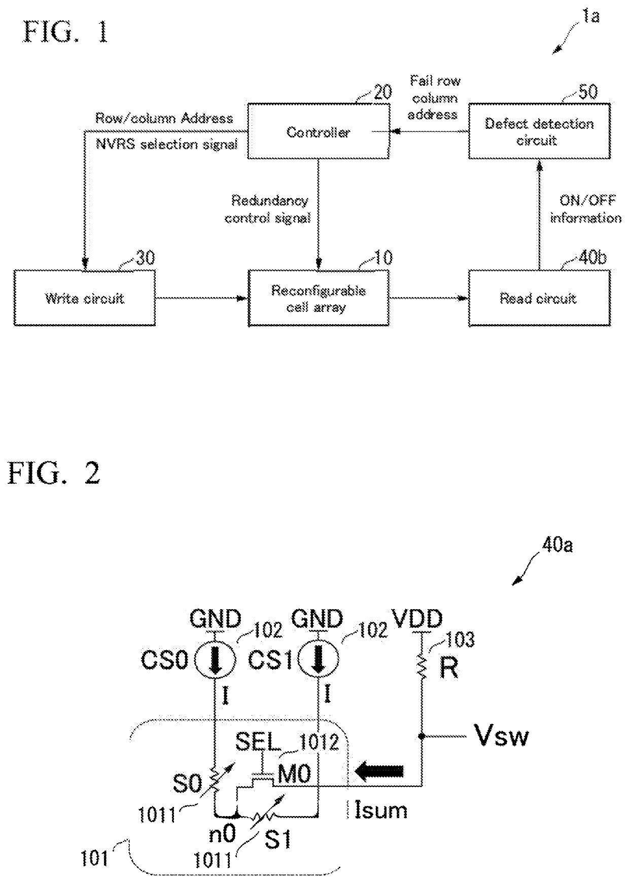
[0042]FIG. 1 shows a structure of the FPGA 1a according to a first exemplary embodiment of the present invention. The FPGA 1a includes a reconfigurable cell array 10, a controller 20, a write circuit 30, a multiple-valued read circuit 40b and a defect detection circuit 50.
[0043]FIG. 2 shows a binary-to-ternary converter circuit 40a according to a first exemplary embodiment of the present invention. The binary-to-ternary converter circuit 40a includes a CNVRS 101, two current sources 102 (CS0 and CS1 shown in FIG. 2), a resistor 103 (R shown in FIG. 2). The CNVRS 101 shown in FIG. 2 is the same as the CNVRS 101 shown in FIG. 12. The CNVRS 101 includes two NVRSs 1011 (S0 and S1 shown in FIG. 2) and a selection transistor 1012 (M0 shown in FIG. 2). Each of the NVRSs 1011 (S0 and S1) includes two terminals. The selection transistor 1012 (M0) includes three terminals named a gate terminal, a source terminal and a drain terminal. The gate terminal is controlled by a select signal SEL. The...
second exemplary embodiment
[0056]Next, a second exemplary embodiment will be described.
[0057]In the first exemplary embodiment, actual ON / OFF state information of the CNVRSs 101 obtained by the multiple-valued read circuit 40b is compared with the original ON / OFF state information of the target application in a defect detection circuit 50 in order to find fail row / column addresses. There is another kind of defect self-detection method [Patent Document 3] only comparing actual ON / OFF state of NVRSs 1011 (S0 and S1 shown in FIG. 15D) each other without comparing the actual ON / OFF state information with the original ON / OFF state information of the target application.
[0058]The defect self-detection principle is that no defect occurs in case that both the NVRSs 1011 (S0 and S1 shown in FIG. 15D) are in the same ON or OFF state, and defect occurs in case that the NVRSs 1011 (S0 and S1 shown in FIG. 15D) are in different states. Typically, it is necessary to read the states of the NVRSs 1011 (S0 and S1 shown in FIG....
PUM
 Abstract
Description
Claims
Application Information