Multiple circuit boards with high-density compression interconnect

a multi-circuit board and compression interconnect technology, applied in the direction of printed circuit details, printed circuit structural associations, printed circuit aspects, etc., can solve the problems of frequency dependence, inability to meet all circuit performance requirements, and inability to meet all circuit performance needs, etc., to achieve the effect of reducing or minimizing costs

Inactive Publication Date: 2021-02-11
SAMTEC
View PDF1 Cites 0 Cited by
  • Summary
  • Abstract
  • Description
  • Claims
  • Application Information

AI Technical Summary

Benefits of technology

[0012]To overcome the problems described above, preferred embodiments of the present invention provide an assembly and a method that provide a PCB architecture that allows separation of the low-speed power / control signals from the high-speed data signals. More specifically, the low-speed power / control signals are routed on a lower-cost PCB constructed of FR-4 or similar material, the high-speed signals are routed on a high-speed PCB using engineered PCB material, and a high-density compression interconnect is used to connect the two PCBs together, which allows a series of PCBs to be connected together as needed to meet design requirements and reduce or minimize cost.

Problems solved by technology

Although FR-4 is a versatile PCB substrate material, it does not satisfy all circuit performance needs.
As these needs and corresponding materials are less common, PCB materials used to provide these specialty requirements are more expensive.
As the dielectric constant determines the signal propagation speed, frequency dependence can introduce phase distortion in wideband applications.
As a result, a PCB with a FR-4 substrate will not meet the needs in many high-speed applications.
Because of the high frequency of the high-speed signals, the PCB 100 needs to be made of high-performance materials, which are expensive.
This results in a more complicated and expensive PCB 100 with compromises in the electrical design.

Method used


Image

  • Multiple circuit boards with high-density compression interconnect
  • Multiple circuit boards with high-density compression interconnect
  • Multiple circuit boards with high-density compression interconnect

Examples


Embodiment Construction

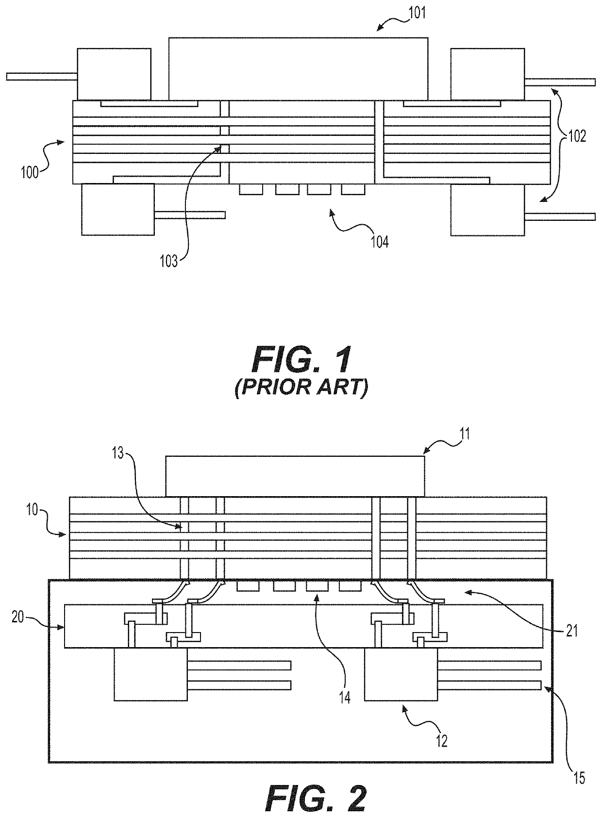
[0030]FIG. 2 shows a preferred embodiment of the present invention that includes two PCBs 10, 20 that are connected together. FIG. 2 shows one power or control, or one power-and-control PCB 10 and one high-speed PCB 20. The power-and-control PCB 10 that routes power and control signals is a simpler and lower cost PCB, for example, and can be constructed of layers of FR-4 substrate material, such as 8-10 layers, or other similar low-cost PCB material, that is in total about 1 mm to about 2 mm thick. As shown in FIG. 2, the top side of the power-and-control PCB 10 can include an integrated circuit (IC) 11 or other components, and the bottom side can include bypass capacitors 14 that can be used with the power supply or other components. PCB 10 and IC 11 can be included in an IC or die package. The IC 11 can be any silicon chip, including, for example, an ASIC or switch IC. The power-and-control PCB 10 includes signal vias 13 that transport signals, such as differential signals, betwee...


PUM


Abstract

A printed circuit board (PCB) assembly includes a first PCB, a high-speed PCB, and a high-speed interconnect electrically and physically connecting the first PCB and the high-speed PCB.

Description

CROSS REFERENCE TO RELATED APPLICATIONS[0001]This application claims the benefit of U.S. Patent Application No. 62 / 644,043 filed on Mar. 16, 2018 and U.S. Patent Application No. 62 / 666,915 filed on May 4, 2018. The entire contents of each application are hereby incorporated by reference.BACKGROUND OF THE INVENTION1. Field of the Invention[0002]The present invention relates to an architecture and a method to electrically and physically connect multiple circuit boards together. More specifically, the present invention relates to connecting a conventional printed circuit board to a high-speed printed circuit board with a high-density compression interconnect.2. Description of the Related Art[0003]A printed circuit board (PCB) is a mechanical substrate that supports and electrically connects electronic components. PCB technology provides a way to reduce the size, weight, and cost of circuitry over previously available point-to-point wiring methods. A PCB uses conductive tracks, traces, ...

Claims


Application Information

Patent Timeline
Patent Type & Authority Applications(United States)
IPC IPC(8): H05K1/14H05K1/11
CPCH05K1/144H05K2201/10189H05K2201/041H05K1/115H05K1/148
Inventor MCMORROW, NORMAN S.GUETIG, KEITH R.SHAH, JIGNESH H.
Owner SAMTEC
Why Eureka
Try Eureka