Display panel and manufacturing method thereof

Active Publication Date: 2021-04-01
WUHAN CHINA STAR OPTOELECTRONICS SEMICON DISPLAY TECH CO LTD
View PDF0 Cites 3 Cited by
  • Summary
  • Abstract
  • Description
  • Claims
  • Application Information

AI Technical Summary

Benefits of technology

The present invention is a display panel and its manufacturing method that has connection lines formed in the display area, instead of in the non-display area. This reduces the width of the non-display area and even achieves a zero non-display area. The technical effect of this invention is that it maximizes the display area and improves the overall appearance and quality of the display.

Problems solved by technology

Therefore, the non-display area NA is required to have a certain width, resulting in a noticeable bezel of the display panel.

Method used


Image

  • Display panel and manufacturing method thereof
  • Display panel and manufacturing method thereof
  • Display panel and manufacturing method thereof

Examples


Embodiment Construction

[0025]The following descriptions for the respective embodiments are specific embodiments capable of being implemented for illustrations of the present invention with referring to appended figures.

[0026]In the accompanied drawing, same numerals are applied to identical elements. It should be understandable that terms like “first,”“second,” etc. are for reference only. They do not imply preference or priority among the referred elements.

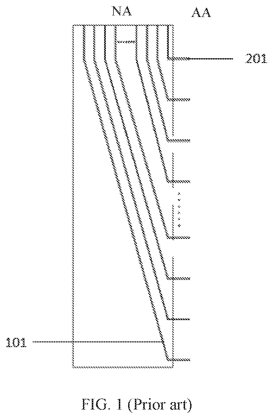
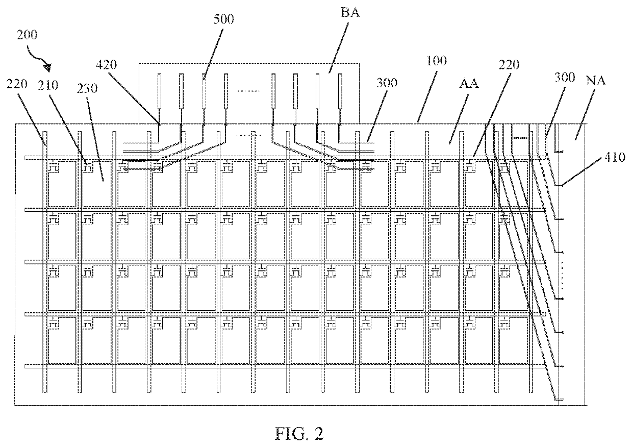
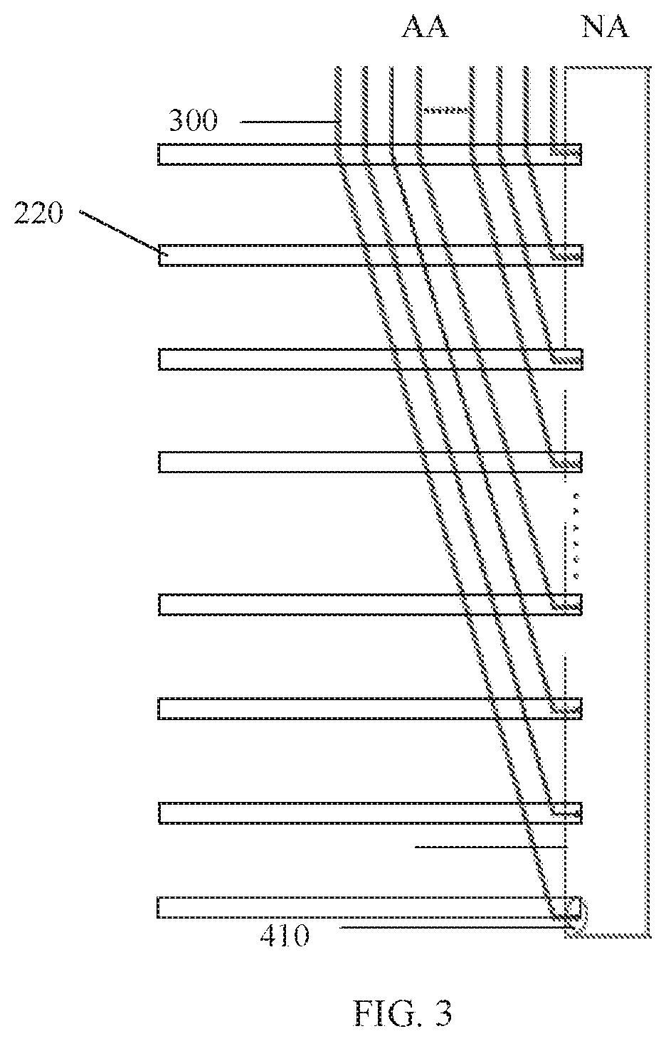
[0027]FIG. 2 is a top view diagram showing a display panel according to an embodiment of the present invention. FIG. 3 is a top view diagram showing the connection of connection lines and signal lines of the display panel of FIG. 2. FIG. 3 is a top-view diagram showing the connection of connection lines and signal lines of the display panel of FIG. 2. FIG. 4 is a sectional diagram showing the connection of connection lines and signal lines of the display panel of FIG. 2. FIG. 5 is a top-view diagram showing the connection of connection lines and bondin...


PUM


Abstract

A display panel includes a substrate, a thin film transistor (TFT) layer on the substrate, and multiple connection lines disposed between the substrate and the TFT layer. The TFT layer includes TFTs and signal lines connected to the TFTs for providing signals to the TFTs. Each connection line is electrically connected to a signal line. The present invention also teaches a display panel manufacturing method. The present invention has the connection lines formed in the display area, instead of in the non-display area, thereby reducing the width of the non-display area.

Description

FIELD OF THE INVENTION[0001]The present invention is generally related to the field of display technology, and more particularly to a display panel and a related manufacturing method.BACKGROUND OF THE INVENTION[0002]Full-screen displays have become the mainstream product. To conform to this trend, manufacturers have adopted various designs to reduce the width of the so-called non-display area of the display panel. Techniques such as gate on array (GOA) have effectively fulfilled the demand for small-bezel displays.[0003]FIG. 1 is a top-view diagram showing a layout of connection lines of a conventional display panel. As shown in FIG. 1, signal lines 201 such as data lines, Vint lines (for voltage transmission), and gate lines of the display area AA are connected to the bonding area through connection lines 101 of the non-display area NA. Therefore, the non-display area NA is required to have a certain width, resulting in a noticeable bezel of the display panel. Especially for a high...

Claims


Application Information

Patent Timeline
IPC IPC(8): H01L27/12
CPCH01L27/124H01L27/1259G02F1/13458G02F1/13452H10K59/131
Inventor FENG, XIAOLIANG
Owner WUHAN CHINA STAR OPTOELECTRONICS SEMICON DISPLAY TECH CO LTD
Why Eureka
Try Eureka