

Ceramic applied electronic device and connector
a technology of electronic devices and connectors, applied in the direction of coupling device connections, measurement devices, instruments, etc., can solve the problems of large force and difficult assembly work, and achieve the effect of good reliability and workability
- Summary
- Abstract
- Description
- Claims
- Application Information
AI Technical Summary
Benefits of technology
Problems solved by technology
Method used
Image

Examples
Embodiment Construction
[0119]Embodiments of this invention will be described with reference to the drawings.
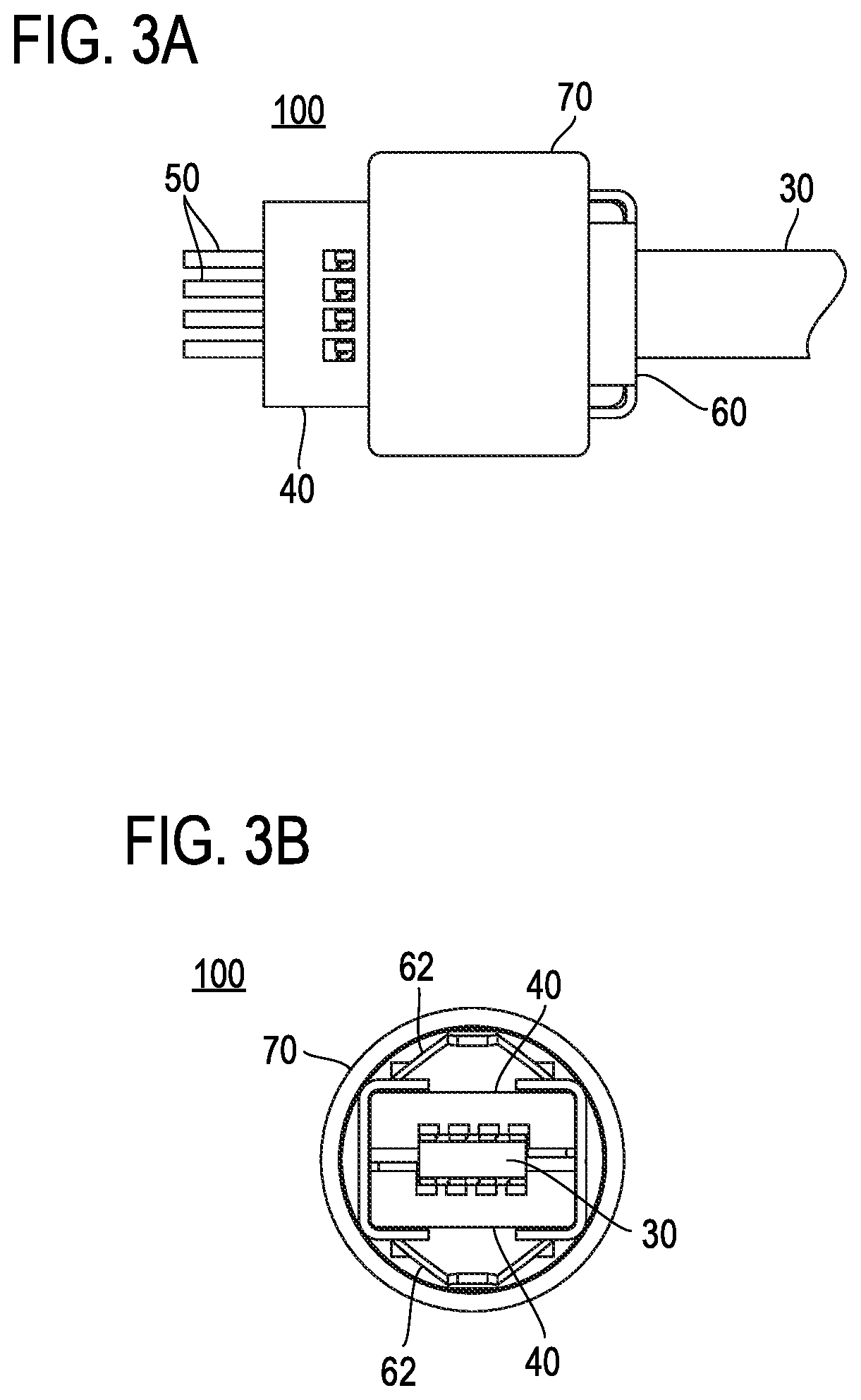
[0120]FIGS. 3A, 3B, 3C, 3D, 4A, and 4B illustrate a connector 100 according to an embodiment. The connector 100 is used to connect a ceramic element incorporated in a ceramic applied electronic device and lead wires for connection with an external apparatus. FIGS. 3A, 3B, 3C, 3D, 4A, and 4B illustrate a state in which a ceramic element 30 is connected to the connector 100.
[0121]The connector 100 includes two insulators 40, eight contacts 50, a spring component 60, and a circular cylindrical sleeve 70 in this example. FIG. 5 is a partial exploded view of the connector 100, and FIGS. 6A and 6B illustrate details of the insulator 40. FIGS. 7A, 7B, and 8 illustrate a state before the ceramic element 30 is connected to the connector 100.
[0122]The two insulators 40 each hold four contacts 50 aligned at a lower surface 40a in this example. The two insulators 40 are arranged such that the lower surface 40a ...
PUM
 Abstract
Description
Claims
Application Information