Channeled lift pin

a lift pin and channel technology, applied in the field of micro-conductor processing or reactor system, can solve the problems of contaminant accumulation on and/or coating the underside of the substrate, and achieve the effect of reducing or preventing unwanted material deposition and/or deposition patterns

Pending Publication Date: 2021-07-08
ASM IP HLDG BV
View PDF3 Cites 114 Cited by
  • Summary
  • Abstract
  • Description
  • Claims
  • Application Information

AI Technical Summary

Benefits of technology

[0006]In some embodiments, a reactor system is provided. The reactor system disclosed herein may allow seating and/or flatt...

Problems solved by technology

During operation of the reactor system comprising dual chambers, undesirable contaminants may accumulate on and/or coat an underside of the substrate (i.e., th...

Method used


Image

  • Channeled lift pin
  • Channeled lift pin
  • Channeled lift pin

Examples


Embodiment Construction

[0028]Although certain embodiments and examples are disclosed below, it will be understood by those in the art that the disclosure extends beyond the specifically disclosed embodiments and / or uses of the disclosure and obvious modifications and equivalents thereof. Thus, it is intended that the scope of the disclosure should not be limited by the particular embodiments described herein.

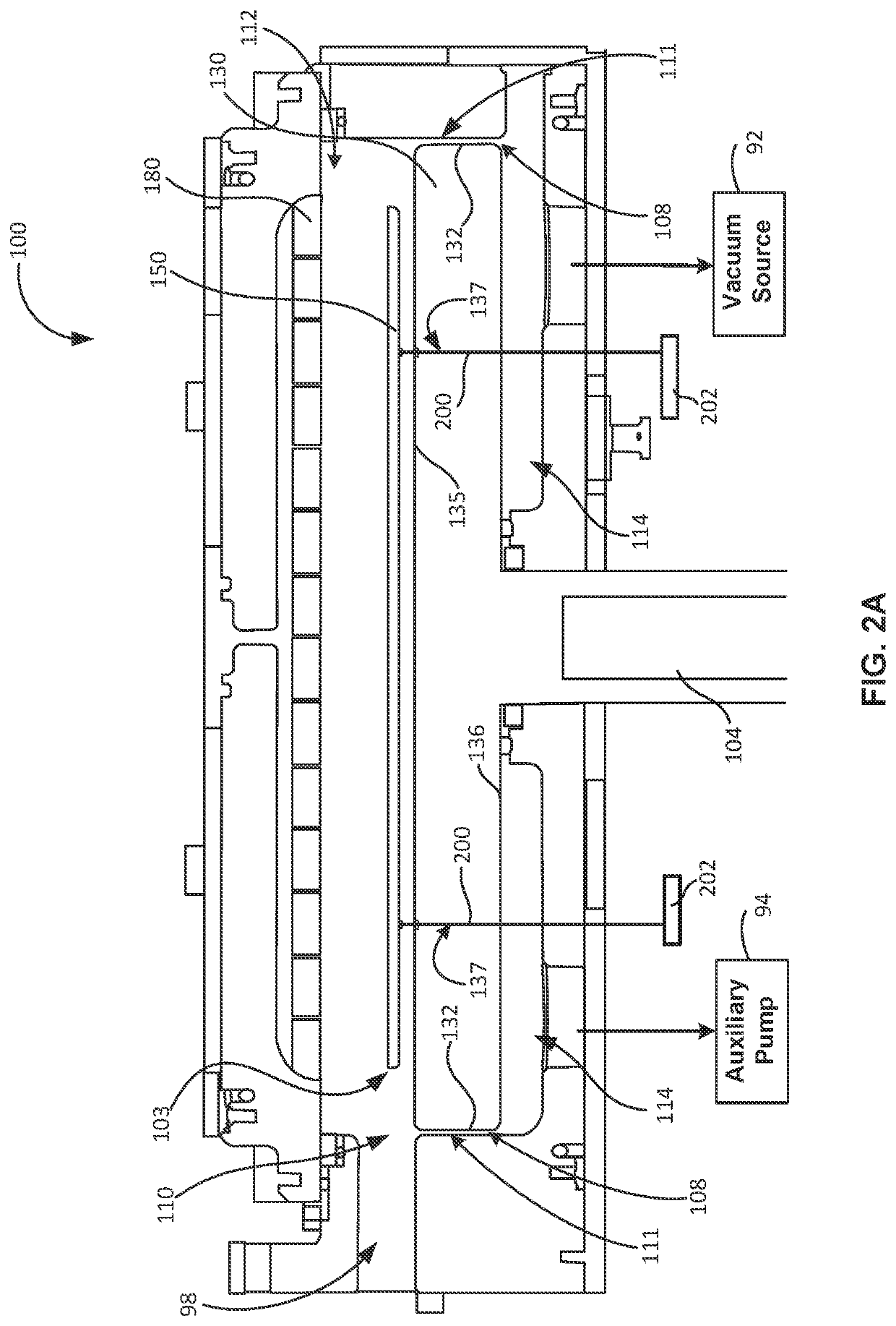
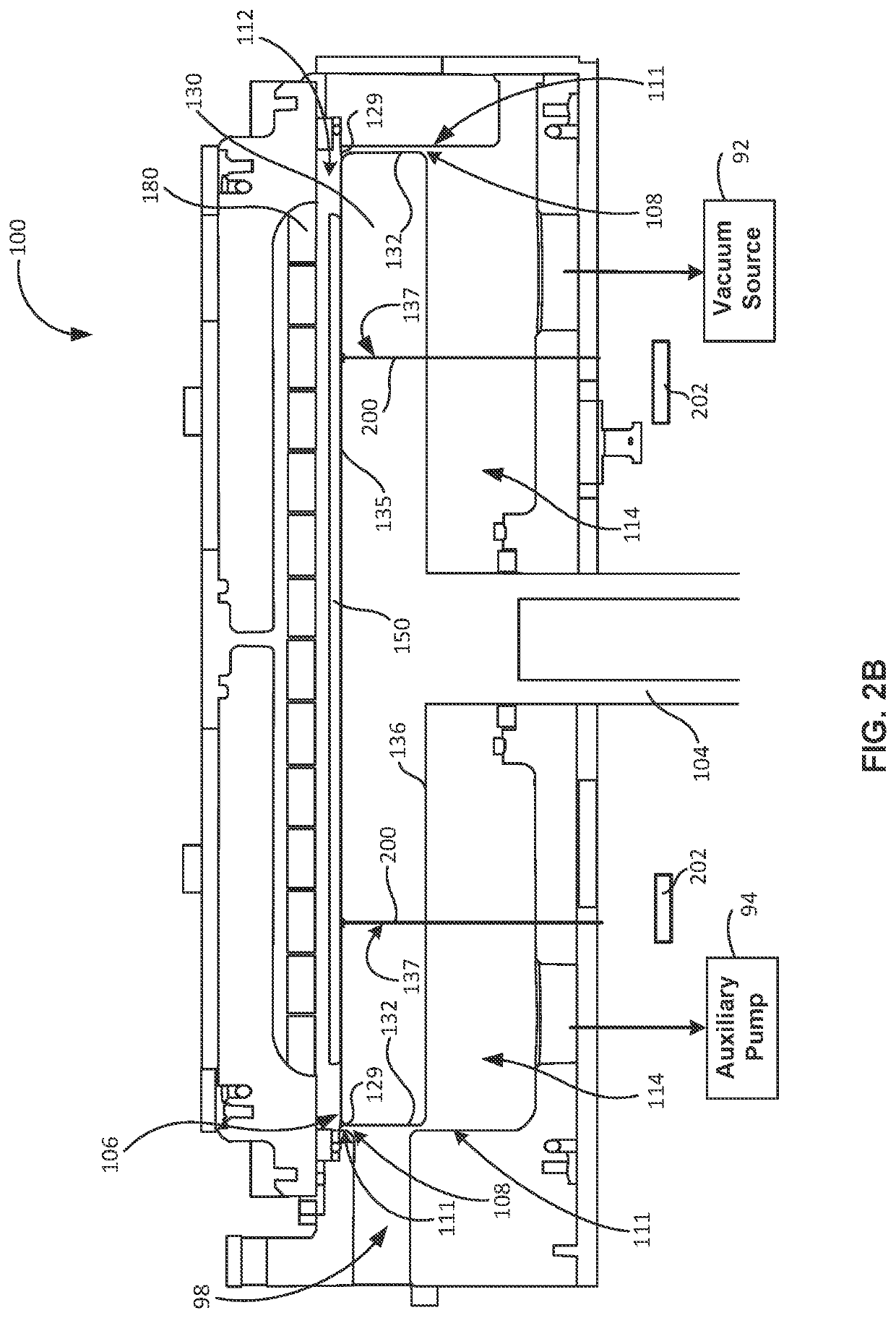
[0029]The illustrations presented herein are not meant to be actual views of any particular material, apparatus, structure, or device, but are merely representations that are used to describe embodiments of the disclosure.

[0030]As used herein, the term “substrate” may refer to any underlying material or materials that may be used, or upon which, a device, a circuit, or a film may be formed.

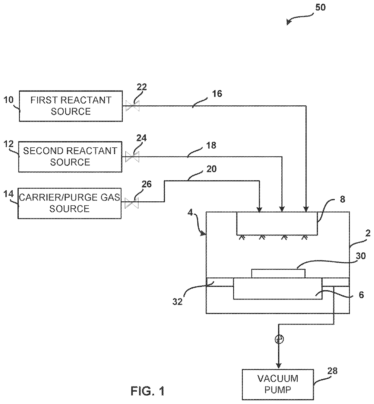
[0031]As used herein, the term “atomic layer deposition” (ALD) may refer to a vapor deposition process in which deposition cycles, preferably a plurality of consecutive deposition cycles, are conducted in a proces...


PUM

PropertyMeasurementUnit
Lengthaaaaaaaaaa
Pressureaaaaaaaaaa
Flow rateaaaaaaaaaa

Abstract

A reactor system may comprise a reaction chamber enclosed by a chamber sidewall, and a susceptor disposed in the reaction chamber between a reaction space and a lower chamber space comprised in the reaction chamber. The susceptor may comprise a pin hole disposed through the susceptor such that the pin hole is in fluid communication with the reaction space and the lower chamber space, and such that the reaction space is in fluid communication with the lower chamber space. A lift pin may be disposed in the pin hole. The lift pin may comprise a pin body comprising a pin channel, defined by a pin channel surface, disposed in the pin body such that the reaction space is in fluid communication with the lower chamber space when the lift pin is disposed in the pin hole.

Description

CROSS-REFERENCE TO RELATED APPLICATIONS[0001]This application is a Non-provisional of, and claims priority to and the benefit of, U.S. Provisional Patent Application No. 62 / 957,516, filed Jan. 6, 2020 and entitled “CHANNELED LIFT PIN,” which is hereby incorporated by reference herein.FIELD OF THE DISCLOSURE[0002]The present disclosure relates generally to a semiconductor processing or reactor system, and particularly a semiconductor reactor system, and components comprised therein, which prevents material deposition on undesirable locations of, for example, the reactor system and / or a substrate.BACKGROUND OF THE DISCLOSURE[0003]Reaction chambers may be used for depositing various material layers onto semiconductor substrates. A semiconductor may be placed on a susceptor inside a reaction chamber. Both the substrate and the susceptor may be heated to a desired substrate temperature set point. In an example substrate treatment process, one or more reactant gases may be passed over a h...

Claims


Application Information

Patent Timeline
IPC IPC(8): H01L21/687H01L21/683
CPCH01L21/68742H01L21/6838C23C16/4586C23C14/50H01L21/67017H01L21/68785C23C16/4583C23C16/4412
Inventor SINGU, GOVINDARAJASEKHARNANDWANA, DINKARDUNN, TODD ROBERTSWAMINATHAN, SHANKARZOPE, BHUSHANWHITE, CARL LOUIS
Owner ASM IP HLDG BV
Why Eureka
Try Eureka