Method and system to calibrate a camera clock using flicker

a technology of camera clock and flicker, applied in the field of digital devices, can solve the problems of affecting image analysis algorithms, high frequency of lighting, etc., and achieve the effect of reducing flickering phenomena in electronic devices and high degree of synchronization

Active Publication Date: 2021-08-19
DSP GROUP
View PDF1 Cites 3 Cited by
  • Summary
  • Abstract
  • Description
  • Claims
  • Application Information

AI Technical Summary

Benefits of technology

[0003]The present invention discloses a method operable on a computerized circuitry employing an image sensor, designed to capture multiple images in a succession. Said method can be utilized to synchronize the clock rate, also known as clock cycle rate, of a device's circuitry with the frequency of a full cycle of the illumination modulation which in some cases may be caused by the main power line frequency. Synchronizing the clock rate with the frequency of a full cycle of said illumination modulation may be utilized in diverse operational tasks in electronic devices, for example, mitigating the flickering phenomena in electronic devices. In some cases, the circuitry may be connected or implemented to electronic devices such as cellular telephones, cameras, video cameras, web cameras, computers, CIS, and the like, requiring high degree of synchronization between the clocks of the communicating devices.
[0013]In some embodiments of the present invention the measured image intensity variability value can be utilized to compute the estimated integration clock counts yielding the estimated lowest image intensity variability value. In some cases, the estimated lowest image intensity variability value can be as the lowest image intensity variability value among the computed variability values. For example, image intensity variability value of the first 20 image frames and the second 20 image frames may be utilized to identify whether the first set of 20 image frames or the second set of 20 image frames has the lower variability value, wherein the variability value is a numeric value indicate the level of light intensity of a captured frame. In some cases, additional sets of image frames, at different pixel integration timings may be measured and utilized to identify the estimated clock rate required to reach to the lowest point of the variability in a set of pixel arrays. The identified number of clock cycles required to reach to the lowest point of the intensity variation in the pixel arrays may be utilized by the circuitry to determine the required clock rate. Thus, the length of a pixel integration time may be synchronized with the frequency of the illumination modulation by adjusting length of a pixel integration time through changing the clock rate of the electronic device. In some cases, the frequency of the illumination modulation may be caused by the main power line frequency. In some cases, setting the number of clock cycles of the pixel integrating time may mitigate the flickering phenomena caused by illumination frequency and a video movie may be seen essentially steady to the average human observer.
[0014]In some cases, accuracy of the circuitry clock may also be necessary for diverse aspects of the circuitry operations such as interfacing with external devices such as digital processors which mandate accurate synchronization between the clock rate of the circuitry processor and the external device. Thus, using the illumination modulation to improve the accuracy of the circuitry processor clock can reduce the requirement for on-board high accuracy clocks which can be expensive and / or complicated, or the need for a high accuracy external clock.

Problems solved by technology

However, electronic devices such a cellular telephones, cameras, and computers which are configured to capture multiple images in a rapid manner, may be impacted by this high frequency of lighting.
The results in some cases may be a flickering effect in the digital image display, and in other cases may negatively impact image analysis algorithms.

Method used


Image

  • Method and system to calibrate a camera clock using flicker
  • Method and system to calibrate a camera clock using flicker
  • Method and system to calibrate a camera clock using flicker

Examples


Embodiment Construction

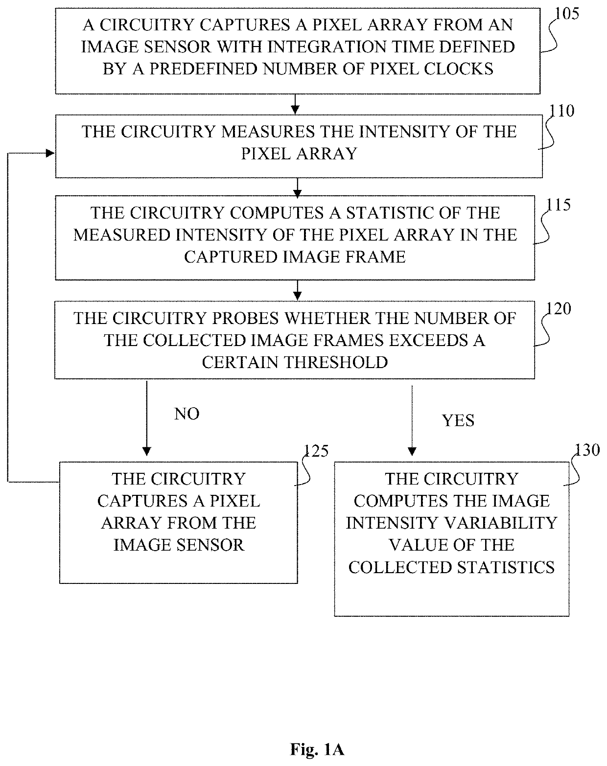
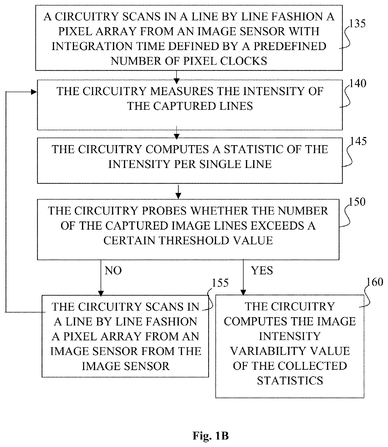
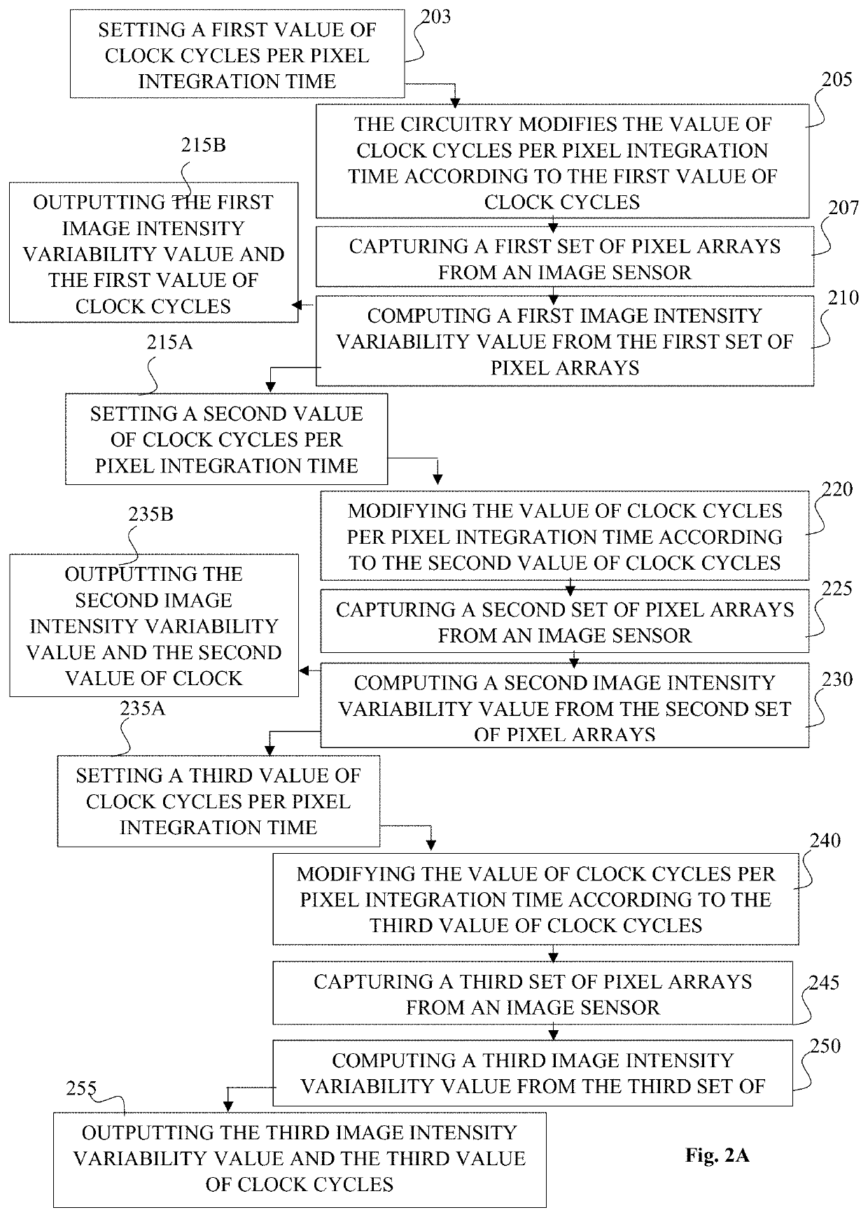
[0027]The present invention discloses a method operable on a circuitry within an image sensor, wherein the circuitry may be implemented or connected to electronic devices and designed to capture multiple images or lines by the image sensor. Such an image sensor can comprise a photosensitive cell array designed to transduce optical image of objects formed on the photosensitive cell array by incidence of light, into corresponding electronic signals, denoted herein as a captured image frame, representing the image captured by the image sensor.

[0028]The method disclosed by the present invention is designed to utilize image intensity variability value to synchronize the clock rate of the electronic device by ensuring that the number of clock cycles per pixel integration time may be synchronized, hence occur at the same rate as the frequency of the illumination frequency.

[0029]The term “clock rate” refers to the frequency at which a processor such as a central processing unit is running. ...


PUM


Abstract

A method operable by circuitry including an image processor, an image sensor, and another clock-dependent device, including measuring a flicker using the image sensor, adjusting a clock rate of the circuitry according to the measured flicker, and operating the clock-dependent device using the adjusted clock rate.

Description

FIELD OF THE INVENTION[0001]The present invention relates to digital devices such as CMOS image sensors (CSI) utilized for acquiring images under artificial illumination presenting non-uniform exposure of consecutive images when the CSI's clock and the illumination frequencies are imperfectly matched.BACKGROUND OF THE INVENTION[0002]Many illumination devices, including incandescent light bulbs, fluorescent lamps, and LED lamps that are fed from the mains current provide an illumination that fluctuates, usually at double the frequency of the mains power, that is, 100 Hz where the current is 50 Hz, and 120 Hz where the current is supplied at 60 Hz. The impact of the periodic changes in the power supply on the illumination devices may not be detected or recognized by the human eye. However, electronic devices such a cellular telephones, cameras, and computers which are configured to capture multiple images in a rapid manner, may be impacted by this high frequency of lighting. The resul...

Claims


Application Information

Patent Timeline
Patent Type & Authority Applications(United States)
IPC IPC(8): H04N13/296H04N17/00G06T7/80
CPCH04N13/296G06T7/85H04N17/002H04N5/04H04N23/745H04N23/71H04N23/73H04N25/53
Inventor SMILANSKY, ZEEVKIMHI, TOMER
Owner DSP GROUP
Why Eureka
Try Eureka