
Graphene channel silicon carbide power semiconductor transistor
a silicon carbide and semiconductor technology, applied in the direction of semiconductor devices, basic electric elements, electrical equipment, etc., can solve the problems of large off-state leakage current, low breakdown voltage, low reliability, etc., and achieve the effect of reducing the overall off-state leakage current, enhancing the function of assisting depletion, and improving breakdown voltag
- Summary
- Abstract
- Description
- Claims
- Application Information
AI Technical Summary
Benefits of technology
Problems solved by technology
Method used
Image

Examples
example 1
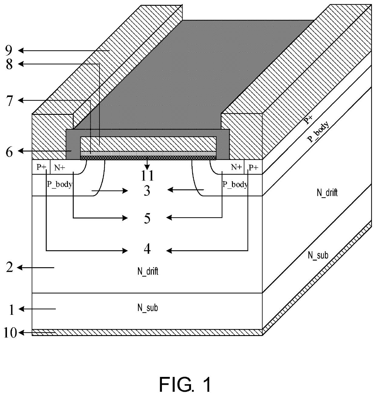
[0034]A graphene channel silicon carbide power semiconductor transistor comprises an N-type substrate 1, wherein one side of the N-type substrate 1 is provided with a drain metal 10, and the other side is an N-type drift region 2, a pair of P-type body regions 3 are arranged at two ends of the N-type drift region 2, a P+-type body contact region 4 and an N+-type source region 5 are respectively arranged in each of the P-type body regions 3, a gate oxide layer 7 is arranged on a surface of the N-type drift region 2, and two ends of the gate oxide layer 7 are respectively extended into the P-type body regions 3 at the two sides, a polysilicon gate 8 is arranged on a surface of the gate oxide layer 7, a passivation layer 6 is arranged on the polysilicon gate 8, and the passivation layer 6 wraps two sides of the polysilicon gate 8, and a source metal 9 is arranged on the N+-type source region 5 and the P+-type body contact region 4.
[0035]In the present embodiment: graphene embedded in t...
example 2
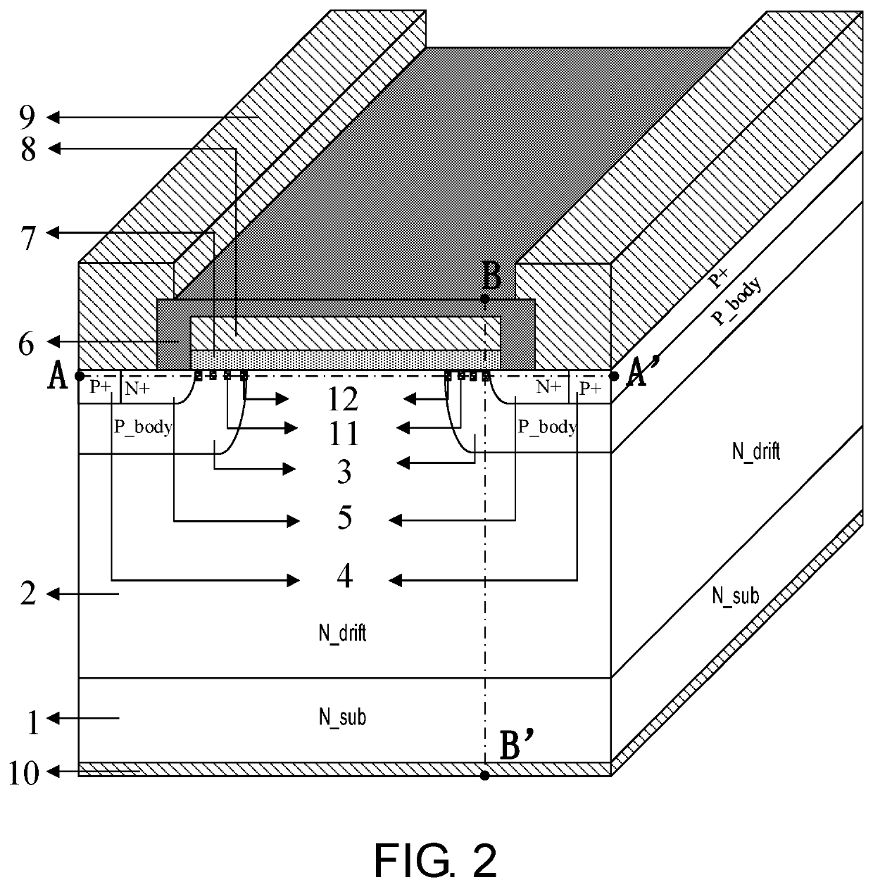
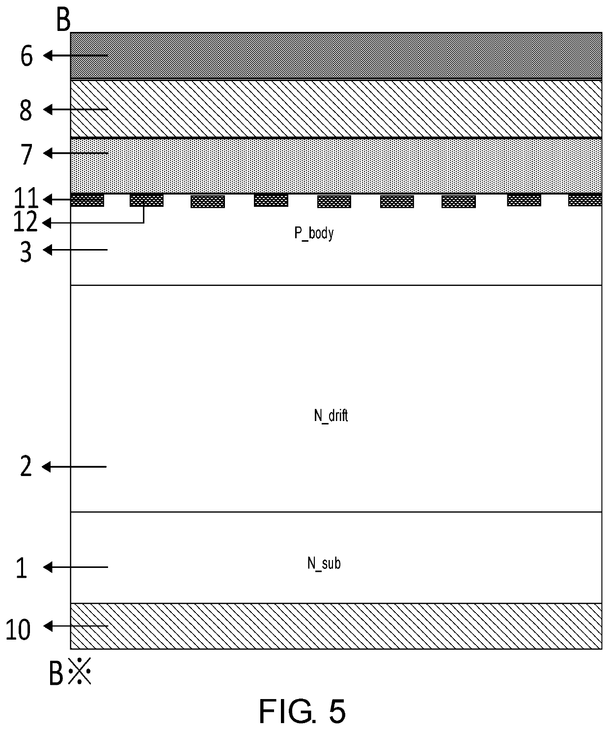
[0036]In the present embodiment, based on a traditional device structure, graphene embedded in the P-body region 3 is extended from an intersection of the N+-type source region 5 and the P-body region 3 to the N-type drift region 5 at intervals in a gate length direction, and a graphene block 12 has a length of 0.1 μm, an interval of 0.1 μm, and a thickness of 1 nm; and a graphene strip 11 is distributed continuously or at intervals in a gate width direction.
[0037]Compared with the device in the Example 2 with graphene distributed continuously or at intervals, the device in the first embodiment in cellular distribution with graphenes interconnected in the gate width direction has a lower on-resistance and a stronger current transmission capability. The cellular graphene makes a gap between the P-type body regions more obvious, an assisting depletion effect stronger, an off-state leakage current smaller, and a breakdown voltage higher. Therefore, the graphene channel silicon carbide ...
PUM
| Property | Measurement | Unit |
|---|---|---|
| gate voltage | aaaaa | aaaaa |
| gate voltage | aaaaa | aaaaa |
| thickness | aaaaa | aaaaa |
Abstract
Description
Claims
Application Information