Wafer-yields and write-qos in flash-based solid state drives

Active Publication Date: 2022-01-13
SK HYNIX INC
View PDF2 Cites 0 Cited by
  • Summary
  • Abstract
  • Description
  • Claims
  • Application Information

AI Technical Summary

Benefits of technology

The patent describes a method for managing bad blocks in flash memory to improve reliability and performance. The invention provides a mechanism to reduce overprovisioning and write amplification, which can degrade the memory device. By identifying and using bad blocks as write-buffers, the method also improves write quality-of-service and reduces bit-error rates of read operations. Additionally, the invention includes techniques to cluster the block types and program the degraded block. Overall, the method improves the reliability and performance of flash memory devices.

Problems solved by technology

In the conventional method of bad-block management, a single bad page in a block can cause the whole block to be removed from usage.
Reducing overprovision and increasing write amplification can degrade the reliability of the memory device, as explained further below.
In addition, when TLC / QLC blocks degrade during the lifetime of the drive such that they may no longer meet the margin requirement, the SSD firmware can mark these bad blocks and use these bad blocks as additional SLC write-buffers instead of increasing the number of bad blocks.

Method used


Image

  • Wafer-yields and write-qos in flash-based solid state drives
  • Wafer-yields and write-qos in flash-based solid state drives
  • Wafer-yields and write-qos in flash-based solid state drives

Examples


Embodiment Construction

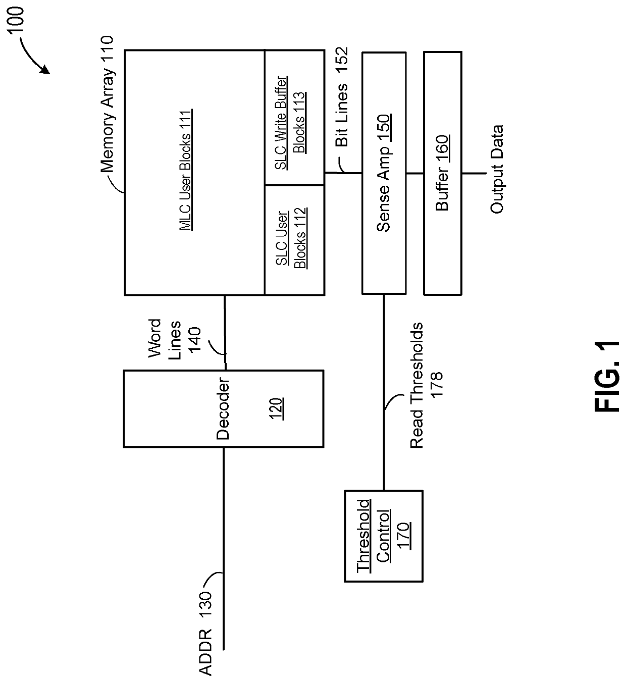
[0021]FIG. 1 is a simplified block diagram of a memory device according to some embodiments of the present invention. In this example, a flash memory device 100 includes a memory cell array 110 having a plurality of non-volatile memory cells. In some embodiments, the memory cells are arranged in a plurality of memory blocks. Each memory block can include multiple non-volatile memory cells, each memory block being associated with a corresponding address. Memory device 100 also includes a decoder 120, for example a row decoder. As an example, decoder 120 receives a command for a memory operation with an address ADDR 130, e.g., a read command with a read address. The address 130 can be a logic address. In an embodiment, the memory operations, such as read, write or program, and erase, etc., are directed to a group of memory cells, for example, a page, a sector, or a block. As described above, a block can include multiple pages. A read or program command is often directed to a page, and...


PUM


Abstract

A non-volatile data storage device includes memory cells arranged in a plurality of blocks and a memory controller coupled to the memory cells for controlling operations of the memory cells. The memory controller is configured to determine if a given block is a bad m-bit multi-level block. In an m-bit multi-level block, each memory cell is an m-bit multi-level cell (MLC), m being an integer equal to or greater than 2. Upon determining that the given block is a good m-bit multi-level block, the memory controller assigns the given block to be an m-bit multi-level user block. Upon determining that the given block is a bad m-bit multi-level block, the memory controller determines if the given block is a good n-bit block. In an n-bit block, each memory cell is an n-bit cell, n being an integer less than m. Upon determining that the given block is a good n-bit block, the memory controller assigns the given block to be an n-bit user block or an n-bit write-buffer block.

Description

BACKGROUND OF THE INVENTION[0001]The present invention relates generally to systems and methods for storage devices, and specifically to improving performance of non-volatile memory devices.[0002]NAND-Flash based solid state drives (SSDs) have better random-read performance compared with magnetic-based hard disk drives (HDDs). However, these drives have low write performance, and the cost per gigabytes (GB) is still approximately 10× higher compared with high capacity HDDs. Improvements in these metrics can increase the total addressable market of SSDs by allowing them to be used in write-heavy and cost-sensitive applications that currently depend on HDDs.[0003]Previous Flash memories are single-level cell (SLC) flash memories, which stores one bit per memory cell. A current approach to reducing cost is to pack more bits per Flash cell, for example, multi-level cell (MLC) Flash memories, to increase the density over SLC Flash memory. However, this approach can reduce the noise-margi...

Claims


Application Information

Patent Timeline
IPC IPC(8): G11C29/44G11C16/04G11C11/56G11C16/10
CPCG11C29/44G11C16/10G11C11/5671G11C16/0483G11C7/02G11C2029/5002G11C11/5628G11C2211/5641G11C2211/5642G11C29/04G06F2212/214G06F12/0246G06F3/064G11C29/765
Inventor BHATIA, AMANZHANG, FAN
Owner SK HYNIX INC
Why Eureka
Try Eureka