
Memory system and method for bad block management

a memory system and bad block technology, applied in the direction of input/output carriers, redundant data error correction, instruments, etc., can solve the problems of degrading the reliability of the memory device, removing the whole block from use, etc., to reduce the overprovision effect, and increase the amount of write amplification

Active Publication Date: 2019-10-03
SK HYNIX INC
View PDF2 Cites 14 Cited by
  • Summary
  • Abstract
  • Description
  • Claims
  • Application Information

AI Technical Summary

Benefits of technology

The invention provides a better way to manage memory blocks that have bad pages. Rather than removing an entire block, the invention allows for a single bad page to trigger additional steps. This can improve reliability and reduce the need for additional memory. The invention also suggests ways to cluster and program degraded blocks more efficiently.

Problems solved by technology

In the conventional method of bad block management, a single bad page in a block can cause the whole block to be removed from usage.
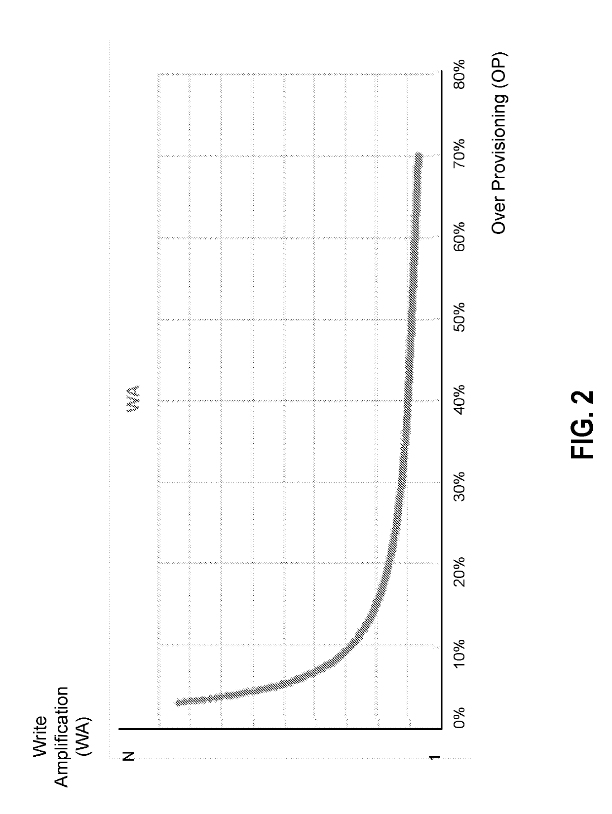
The inventors have recognized that this practice can reduce overprovision (OP) and lead to more write amplification (WA), which can degrade the reliability of the memory device, as explained further below.

Method used


Image

  • Memory system and method for bad block management
  • Memory system and method for bad block management
  • Memory system and method for bad block management

Examples


Embodiment Construction

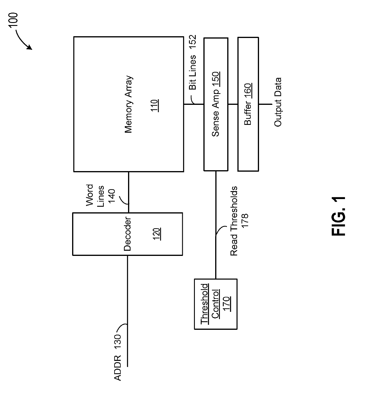
[0024]FIG. 1 is a simplified block diagram of a memory device according to some embodiments of the present invention. In this example, a flash memory device 100 includes a memory cell array 110 having a plurality of non-volatile memory cells. In some embodiments, the memory cells are arranged in a plurality of memory blocks. Each memory block can include multiple non-volatile memory cells, each memory block being associated with a corresponding address. Memory device 100 also includes a decoder 120, for example a row decoder. In an example, decoder 120 receives a command for a memory operation with an address ADDR 130, e.g., a read command with a read address. The address 130 can be a logic address. In an embodiment, the memory operations, such as read, write or program, and erase, etc., are directed to a group of memory cells, for example, a page, a sector, or a block. As described above, a block can include multiple pages. A read or program command is often directed to a page, and...


PUM


Abstract

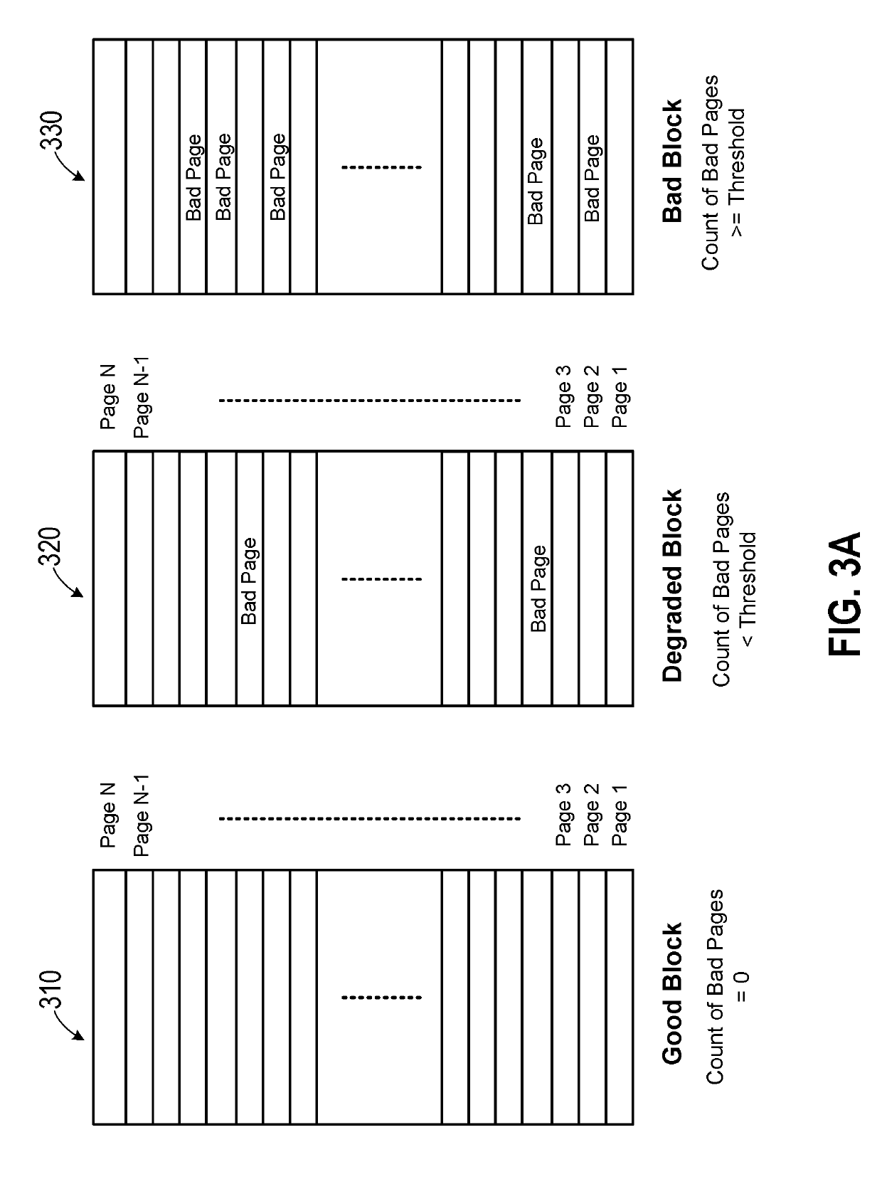
A method is provided for controlling a storage system, which can include a plurality of memory cells arranged in blocks and a memory controller coupled to the plurality of memory cells for controlling data write and read in the plurality of memory cells. The method includes identifying a block as a good block, if a count of bad pages in the block is zero, identifying the block as a degraded block if the count of bad pages is below a threshold number, and identifying the block as a bad block if the count of bad pages is above or equal to the threshold number. The method includes using good blocks and degraded blocks for read and program operations, and not using the bad blocks.

Description

CROSS-REFERENCES TO RELATED APPLICATIONS[0001]The present application claims priority to Provisional Application No. 62 / 652,177 entitled “BAD BLOCK MANAGEMENT,” filed Apr. 3, 2018, which is assigned to the assignee hereof and expressly incorporated by reference herein in its entirety.BACKGROUND OF THE INVENTION[0002]The present invention relates generally to systems and methods for storage devices, and specifically to improving performance of non-volatile memory devices.[0003]Solid-state memory is ubiquitously used in a variety of electronic systems including, for example, consumer electronic devices (e.g., cellular phones, cameras, computers, etc.) and in enterprise computing systems (e.g., hard drives, random access memory (RAM), etc.). Solid-state memory has gained popularity over mechanical or other memory storage techniques due to latency, throughput, shock resistance, packaging, and other considerations. Among these non-volatile memory devices, NAND flash memory devices are po...

Claims


Application Information

Patent Timeline
Patent Type & Authority Applications(United States)
IPC IPC(8): G11C29/38G06F11/10G06F11/14G06F3/06
CPCG06F3/0619G06F11/1471G06F2201/82G11C29/38G06F3/064G06F3/0679G06F11/1004G06F11/1032G06F12/0246G06F13/1668G06F11/108G11C29/44G11C29/883
Inventor CAI, YUZHANG, FANKUMAR, NAVEENBHATIA, AMANXIONG, CHENRONGLU, XUANXUAN
Owner SK HYNIX INC
Learn More