Imaging device, imaging system, and method of driving imaging device

a technology of imaging device and imaging system, which is applied in the direction of color television details, television system details, television systems, etc., can solve the problems of image quality deterioration and error, and achieve the effect of not decreasing the readout speed

Active Publication Date: 2022-04-28
CANON KK
View PDF6 Cites 0 Cited by
  • Summary
  • Abstract
  • Description
  • Claims
  • Application Information

AI Technical Summary

Benefits of technology

[0004]An object of the present invention is to provide a technique for acquiring a high-quality image without decreasing a readout speed in an imaging device that switches a gain of an amplifier circuit for each pixel in accordance with an amount of incident light.

Problems solved by technology

However, when a sample-and-hold circuit is applied to an imaging device that switches the gain of the amplifier circuit for each pixel in accordance with the amount of incident light, an error may occur when a signal of a pixel reset level is read out.
As a result, the level difference of the luminance occurring near the boundary at which the gain of the amplifier circuit is switched cannot be appropriately corrected, and the image quality may deteriorate.

Method used


Image

  • Imaging device, imaging system, and method of driving imaging device
  • Imaging device, imaging system, and method of driving imaging device
  • Imaging device, imaging system, and method of driving imaging device

Examples


first embodiment

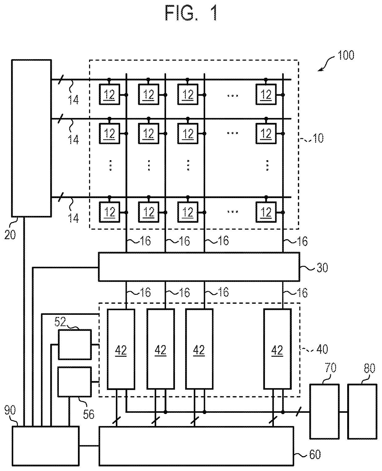
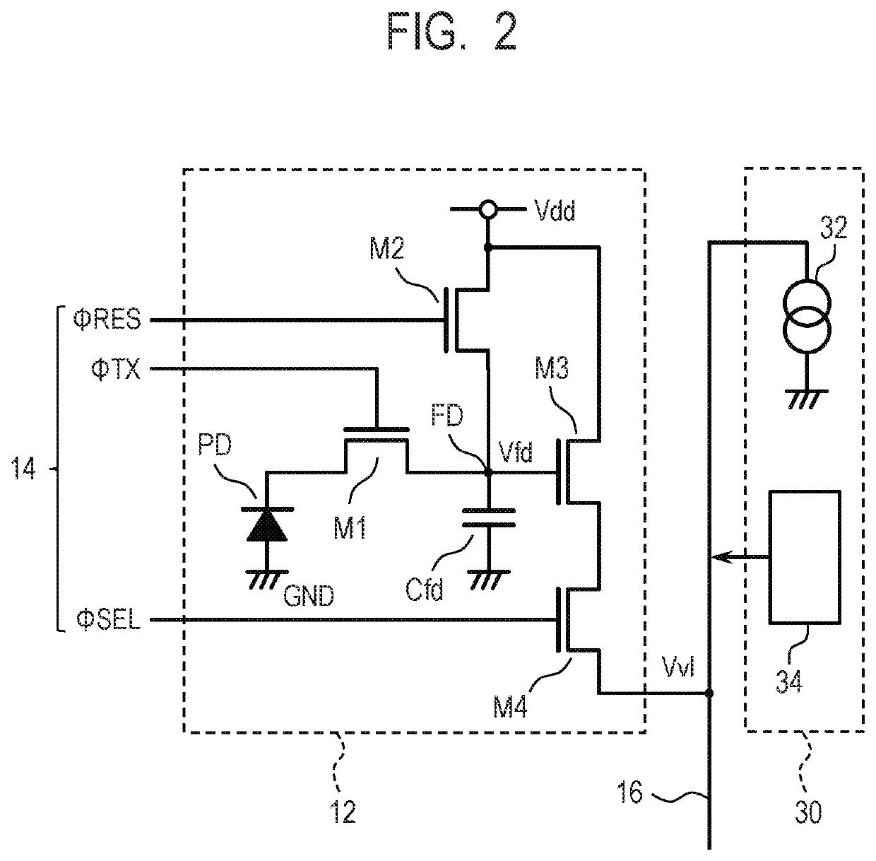
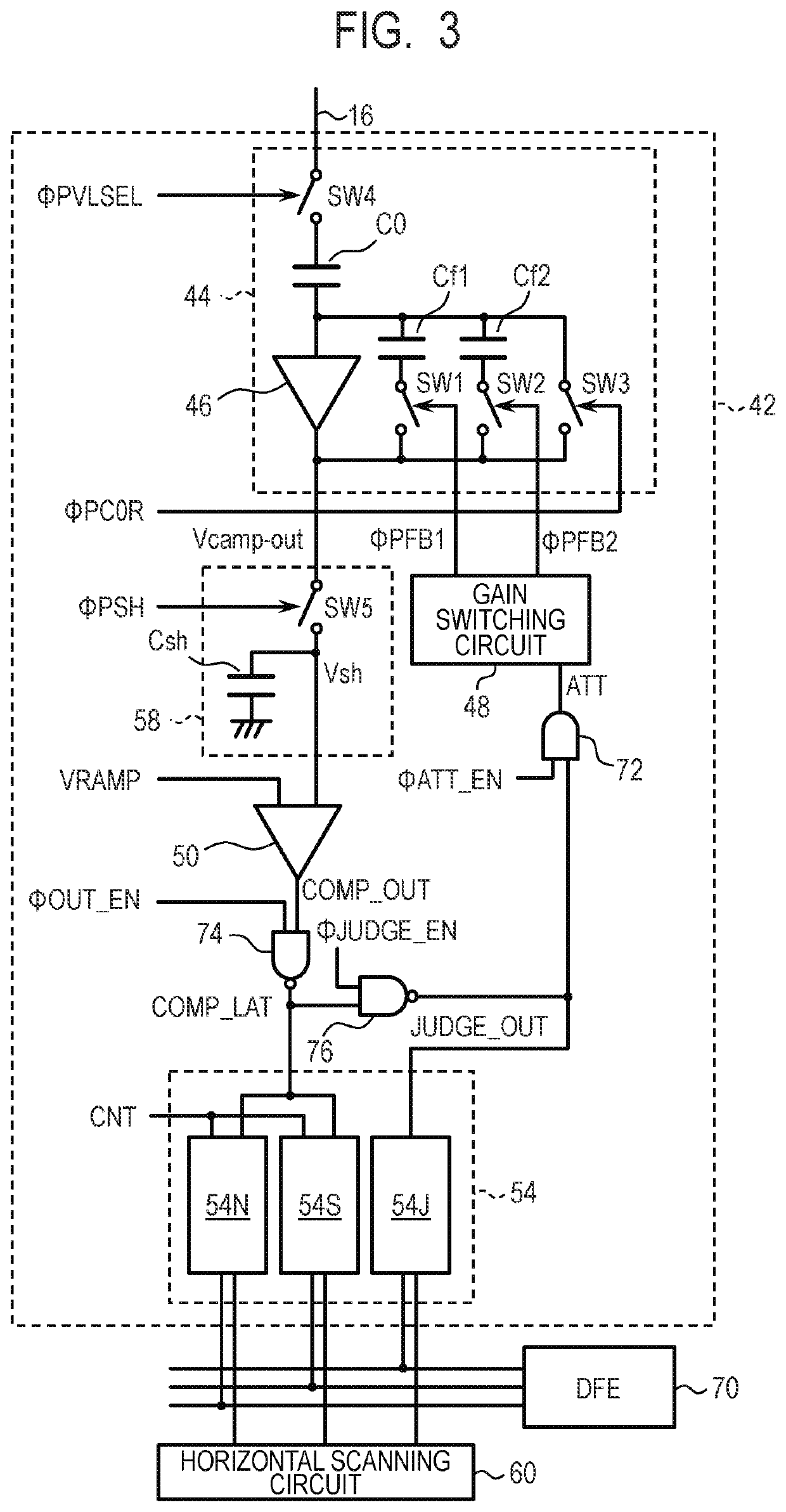
[0023]An imaging device and a method of driving the same according to a first embodiment of the present disclosure will be described with reference to FIG. 1 to FIG. 7. FIG. 1 is a block diagram illustrating a configuration example of an imaging device according to the present embodiment. FIG. 2 is a circuit diagram illustrating a configuration example of a pixel and an output line control unit in the imaging device according to the present embodiment. FIG. 3 is a circuit diagram illustrating a configuration example of a column circuit in the imaging device according to the present embodiment. FIG. 4 and FIG. 7 are timing charts illustrating a method of driving the imaging device according to the present embodiment. FIG. 5 is a graph illustrating a method of correcting a pixel value in the imaging device according to the present embodiment. FIG. 6 is a timing chart illustrating a method of driving the imaging device according to the reference example.

[0024]First, a general configura...

second embodiment

[0131]An imaging device and a method of driving the same according to a second embodiment of the present invention will be described with reference to FIG. 8 and FIG. 9. The same components as those of the imaging device according to the first embodiment are denoted by the same reference numerals, and the description thereof will be omitted or simplified. FIG. 8 is a block diagram illustrating a configuration example of an imaging device according to the present embodiment. FIG. 9 is a circuit diagram illustrating a configuration example of a column circuit in the imaging device according to the present embodiment.

[0132]The imaging device 100 according to the present embodiment is similar to the imaging device according to the first embodiment except that the AD conversion function is not provided. The analog pixel signal acquired by the pixel 12 is output to the outside of the imaging device 100 via the signal output unit 80 without being subjected to AD conversion. An analog pixel...

third embodiment

[0137]A method of driving an imaging device according to a third embodiment of the present invention will be described with reference to FIG. 10 to FIG. 13. The same components as those of the imaging device according to the first and second embodiments are denoted by the same reference numerals, and the description thereof will be omitted or simplified. FIG. 10 and FIG. 11 are schematic diagrams illustrating a method of driving the imaging device according to the present embodiment. FIG. 12 is a timing chart illustrating a method of driving the imaging device according to the reference example. FIG. 13 is a timing chart illustrating the method of driving the imaging device according to the present embodiment.

[0138]In the present embodiment, another method of driving the imaging device according to the first embodiment will be described. That is, in the present embodiment, an operation example in the case where line interleaving driving is performed in which a readout operation of a...


PUM


Abstract

The imaging device includes a pixel including a photoelectric converter, an output line, a readout circuit unit connected to the output line, and a control unit. The readout circuit unit includes an amplifier circuit, a first switch for resetting the amplifier circuit, a sample-and-hold circuit, a second switch provided between the amplifier circuit and the sample-and-hold circuit, and a gain switching circuit. The control unit performs a first period of resetting the amplifier circuit by first switch, and a second period of connecting the amplifier circuit and the sample-and-hold circuit by the second switch. The first and second periods at least partially overlap with each other, and a timing at which the second switch transitions from an on state to an off state in the second period is later than a timing at which the first switch transitions from an on state to an off state in the first period.

Description

BACKGROUND OF THE INVENTIONField of the Invention[0001]The present disclosure relates to an imaging device, an imaging system, and a method of driving the imaging device.Description of the Related Art[0002]As a technique for achieving both a wide dynamic range and high readout speed in an imaging device, a method of switching the gain of an amplifier circuit for each pixel according to an amount of incident light has been proposed. Japanese Patent Application Laid-Open No. 2017-079464 describes a method of correcting a level difference in luminance occurring near a boundary at which a gain of an amplifier circuit is switched. Japanese Patent Application Laid-Open No. 2001-045378 describes a technique for increasing a readout speed by using a sample-and-hold circuit.[0003]However, when a sample-and-hold circuit is applied to an imaging device that switches the gain of the amplifier circuit for each pixel in accordance with the amount of incident light, an error may occur when a signa...

Claims


Application Information

Patent Timeline
Patent Type & Authority Applications(United States)
IPC IPC(8): H04N5/359H04N5/378
CPCH04N5/359H04N5/378H04N25/589H04N25/75H04N25/62
Inventor SUZUKI, ATSUSHIYAMASHITA, TAKANORI
Owner CANON KK
Why Eureka
Try Eureka