Package device and a manufacturing method thereof
- Summary
- Abstract
- Description
- Claims
- Application Information
AI Technical Summary
Benefits of technology
Problems solved by technology
Method used
Image

Examples
first embodiment
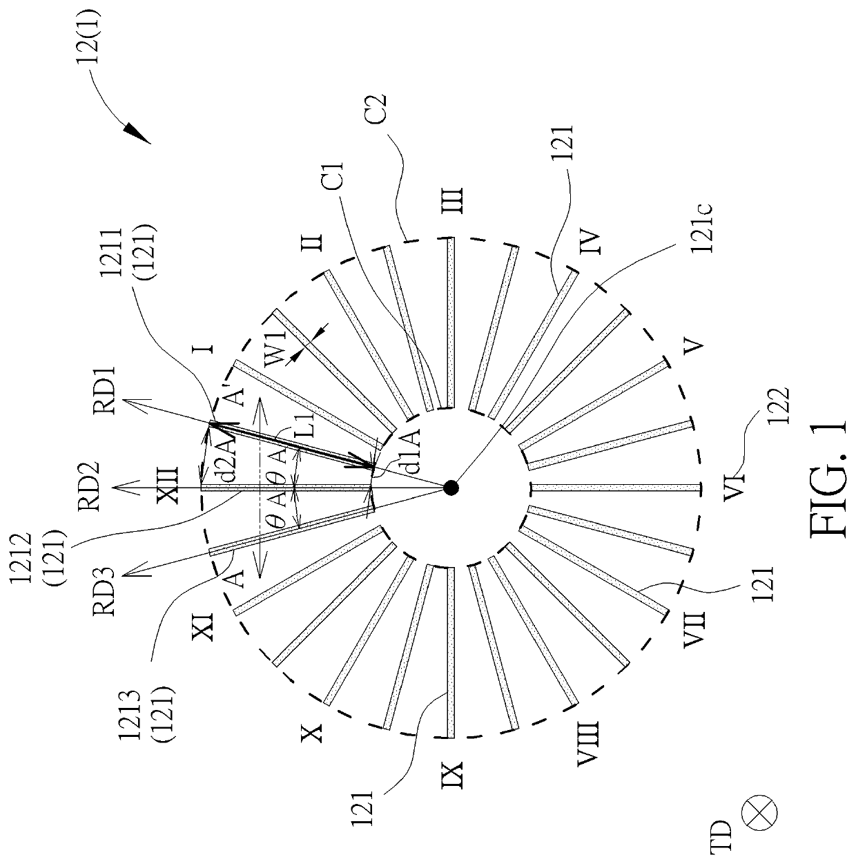
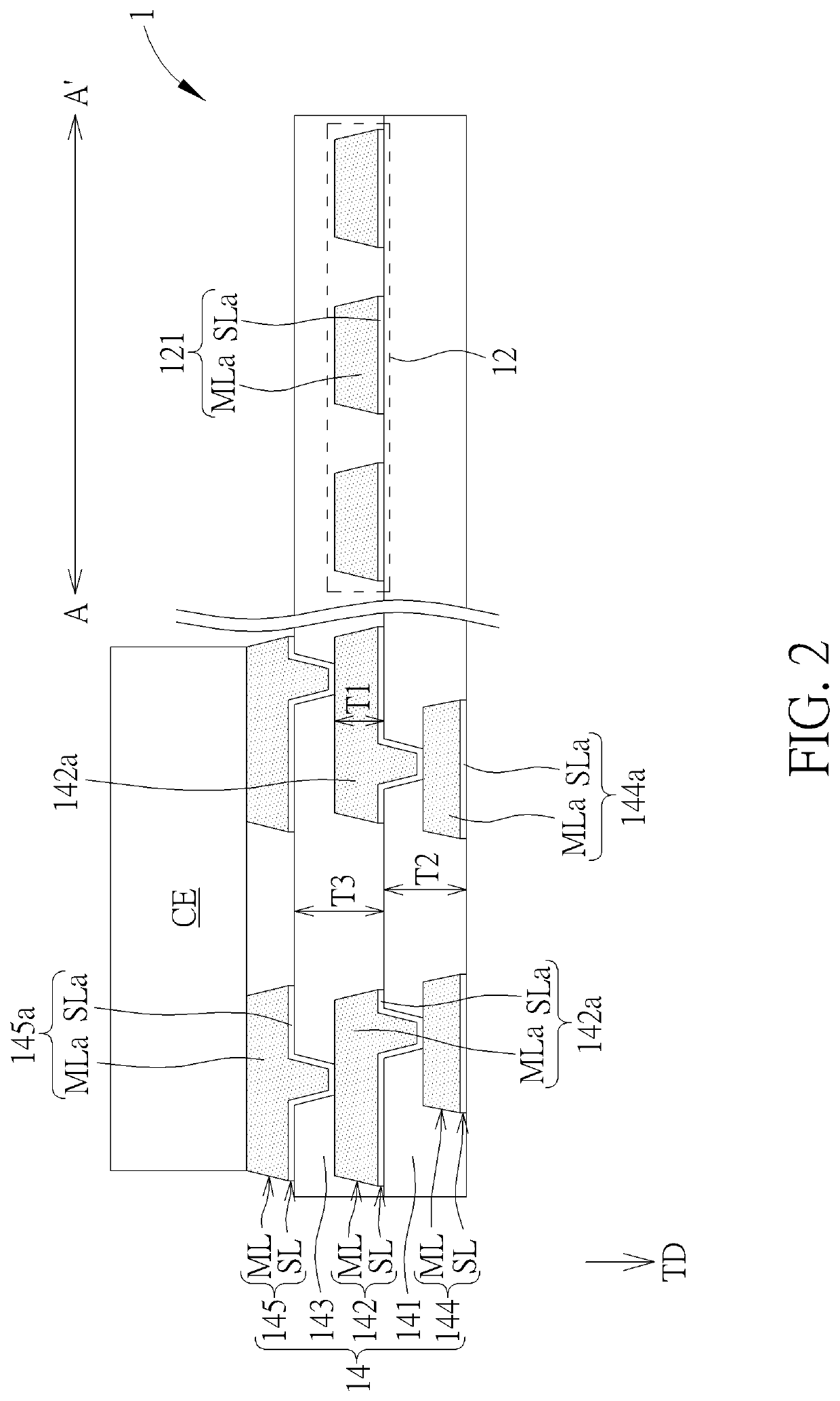
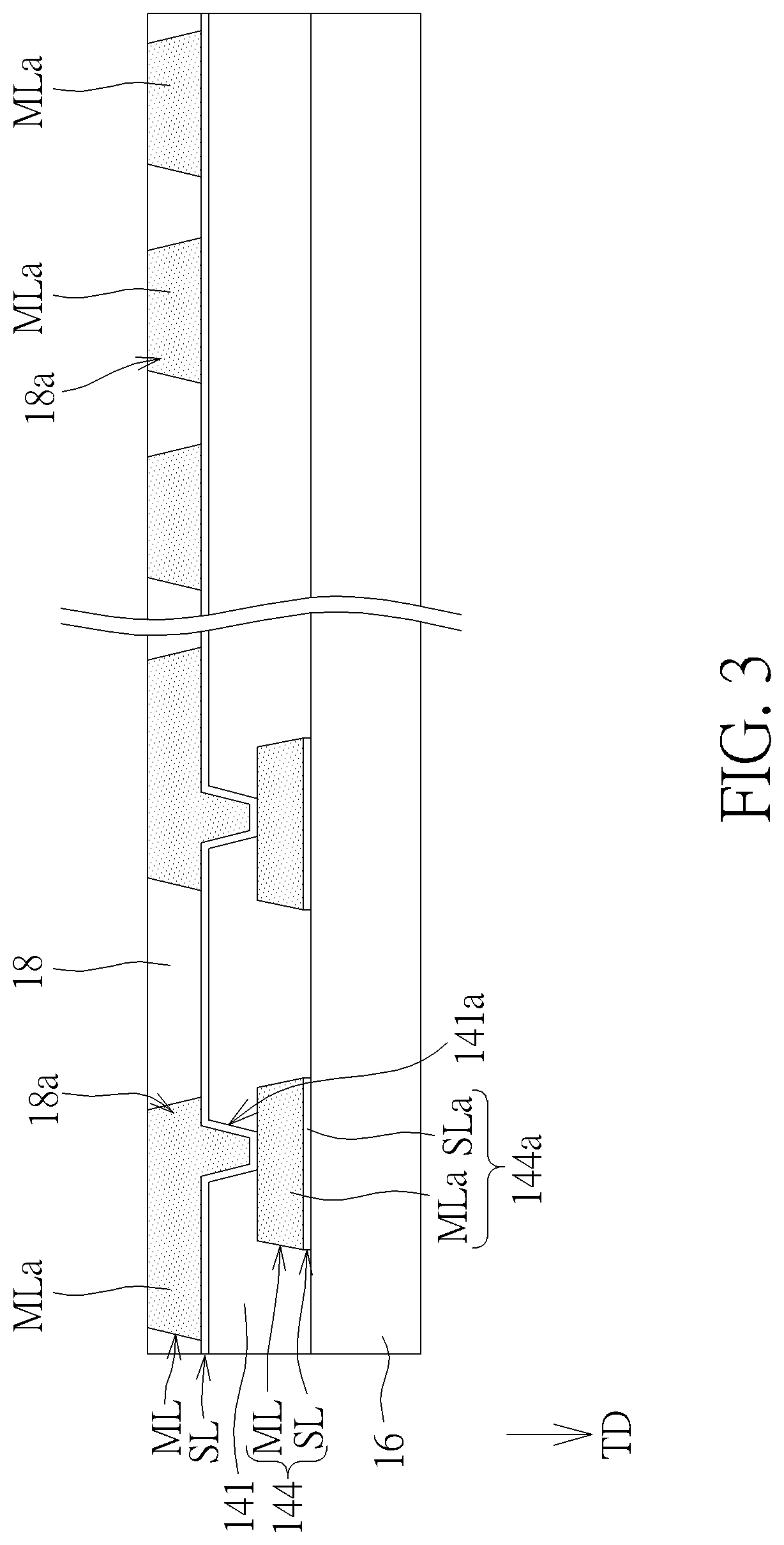
[0040]The following description further details the manufacturing method of the package device of this embodiment. The manufacturing method of the package device of some embodiments of the present disclosure may include providing the carrier 16, and forming the redistribution layer 14 on the carrier 16, in which the redistribution layer 14 may include the first dielectric layer 141, the conductive layer 142, and the second dielectric layer 143. The conductive layer 142 is disposed between the first dielectric layer 141 and the second dielectric layer 143, in which the redistribution layer 14 may have the test mark 12, and the test mark 12 may include a plurality of or at least one conductive pattern 121, and the conductive pattern 121 may be formed of the conductive layer 142. In some embodiments, the plurality of conductive patterns 121 may be arranged in the ring shape, but not limited thereto. For details, refer to FIG. 3 in combination with FIG. 2. FIG. 3 schematically illustrat...
second embodiment
[0049]FIG. 7 schematically illustrates a top view of the test mark of the present disclosure. As shown in FIG. 7, the test mark 22 may include a plurality of conductive patterns 221, and these conductive patterns 221 may have substantially similar top-view shapes. The conductive patterns 221 may be arranged along at least one direction or arranged along multiple directions, for example, along the direction D1 and / or the direction D2. The direction D1 may be different from the direction D2, and the direction D1 may be, for example, perpendicular to the direction D2, but not limited thereto. In some embodiments, the sizes of the plurality of conductive patterns 221 may sequentially increases or decreases, for example, along the at least one direction. It should be noted that the above-mentioned sequential increase or decrease may not mean that the sizes need to be changed proportionally. In some embodiments, the top-view shapes of the conductive patterns 121 may be, for example, an E-...
PUM
 Abstract
Description
Claims
Application Information
 - R&D Engineer
- R&D Manager
- IP Professional
- Industry Leading Data Capabilities
- Powerful AI technology
- Patent DNA Extraction
Browse by: Latest US Patents, China's latest patents, Technical Efficacy Thesaurus, Application Domain, Technology Topic.
© 2024 PatSnap. All rights reserved.Legal|Privacy policy|Modern Slavery Act Transparency Statement|Sitemap