Display device and display device manufacturing method

a display device and manufacturing method technology, applied in the field of display technologies, can solve the problems of increasing the total thickness of the mobile phone, raising the use cost, damage, etc., and achieve the effects of reducing the viewing angle of the display device, lowering the transmittance, and increasing the transmittan

Pending Publication Date: 2022-06-16
WUHAN CHINA STAR OPTOELECTRONICS SEMICON DISPLAY TECH CO LTD
View PDF0 Cites 0 Cited by
  • Summary
  • Abstract
  • Description
  • Claims
  • Application Information

AI Technical Summary

Benefits of technology

The present invention is a display device that includes a layer of electrochromic material. By changing the electrical field applied to the electrochromic layer, the device can switch between different levels of transparency. This allows for higher transparency in a wide view angle mode without affecting the normal display of the device, and lowered transparency in a narrow view angle to protect privacy. The device can switch between modes flexibly, making it suitable for a wider range of applications.

Problems solved by technology

A conventional display device has a technical issue that a plug-in privacy protection film lowers a transmittance of a display screen and certainly influences a display effect, influences display experience in non-public occasions, drastically increases a total thickness of the mobile phone, and easily results in damages to raise a use cost.

Method used


Image

  • Display device and display device manufacturing method
  • Display device and display device manufacturing method
  • Display device and display device manufacturing method

Examples


Embodiment Construction

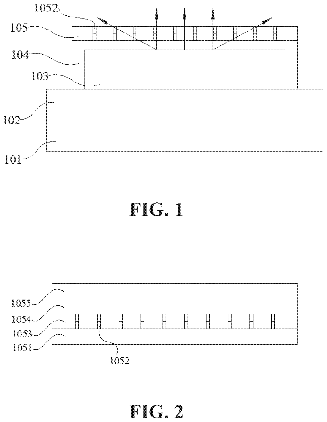
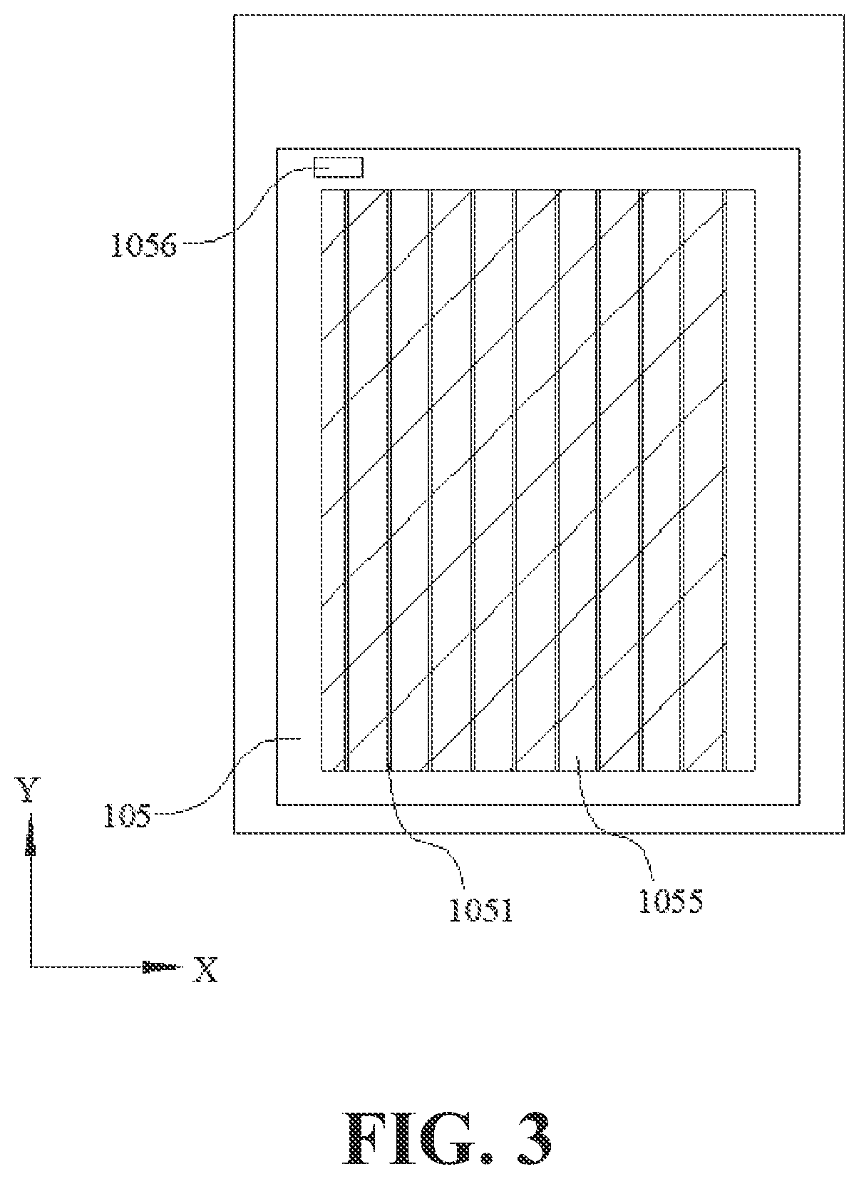
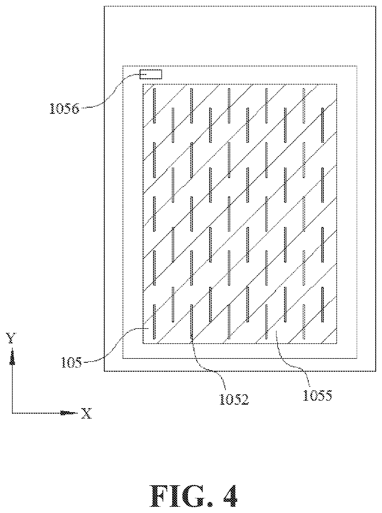
[0045]The technical solution in the embodiment of the present invention will be clearly and completely described below with reference to the accompanying drawings in the embodiments of the present invention. Apparently, the described embodiments are merely some embodiments of the present invention instead of all embodiments. According to the embodiments in the present invention, all other embodiments obtained by those skilled in the art without making any creative effort shall fall within the protection scope of the present invention.

[0046]In the description of the present invention, it should be understood that terminologies “center”, “longitudinal”, “transverse”, “length”, “width”, “thickness”, “upper”, “lower”, “front”, “rear”, “left”, “side”, “vertical”, “horizontal”, “top”, “bottom”, “inner”, “outer”, “clockwise”, “counterclockwise” for indicating relations of orientation or position are based on orientation or position of the accompanying drawings, are only for the purposes of...


PUM

PropertyMeasurementUnit
widthaaaaaaaaaa
viewing angleaaaaaaaaaa
transmittanceaaaaaaaaaa

Abstract

The present invention discloses a display device and a manufacturing method thereof, the display device includes: an underlay substrate; a circuit layer disposed on a side surface of the underlay substrate; a light emitting device layer disposed on a side surface of the circuit layer away from the underlay substrate; an encapsulation layer covering a side surface of the light emitting device layer away from the circuit layer and at least one short side surface of the light emitting device layer; and an electrochromic device layer disposed on a side surface of the encapsulation layer away from the light emitting device layer.

Description

FIELD OF INVENTION[0001]The present invention relates to a field of display technologies, specifically relates to a display device and a display device manufacturing method.BACKGROUND OF INVENTION[0002]With the development of society, people pay more and more attention to the protection of personal privacy, and the harm of privacy leakage is also increasing. At present a viewing angle of a mobile phone is basically near 180°. When a mobile phone is used, in addition the user of the mobile phone uprightly facing the display surface, other people can also clearly see display contents of the mobile phone from two opposite sides of the mobile phone in an angle of view nearly parallel to the display surface of the mobile phones. When a mobile phone is used in public, contents on the mobile phone is easily acquired by other people. Especially in today's highly developed information, mobile phones are used more and more frequently, and the contents on mobile phones become more and more imp...

Claims


Application Information

Patent Timeline
Patent Type & Authority Applications(United States)
IPC IPC(8): G02F1/157
CPCG02F1/157H01L27/156H10K59/50H10K59/12H10K59/1201G02F1/155G02F2201/44
Inventor ZHENG, BINGWEN
Owner WUHAN CHINA STAR OPTOELECTRONICS SEMICON DISPLAY TECH CO LTD
Why Eureka
Try Eureka