Light emitting display device with integrated touch screen and method of manufacturing the same

Pending Publication Date: 2022-06-16
LG DISPLAY CO LTD
View PDF8 Cites 1 Cited by
  • Summary
  • Abstract
  • Description
  • Claims
  • Application Information

AI Technical Summary

Benefits of technology

This patent is about a display device with a touch screen that has a hole pattern. This hole pattern is formed by two layers of material that are stacked on top of each other. The bottom layer is concave, and the top layer is convex. The device also has an organic encapsulation layer that fills the hole pattern, but it doesn't apply to a specific area where the touch pad is connected. This helps prevent any defects that could occur in the connection between the routing and link lines, which makes the device more reliable.

Problems solved by technology

This contact area is located outside a dam formed in a non-display area of the display device, and there is a defect, in which an organic encapsulation layer included in the encapsulation film of the display device passes over the dam and is applied up to a contact area of a routing line and a link line of a touch pad, so that the signals of the touch driving element are not transmitted to the touch screen.

Method used


Image

  • Light emitting display device with integrated touch screen and method of manufacturing the same
  • Light emitting display device with integrated touch screen and method of manufacturing the same
  • Light emitting display device with integrated touch screen and method of manufacturing the same

Examples


Embodiment Construction

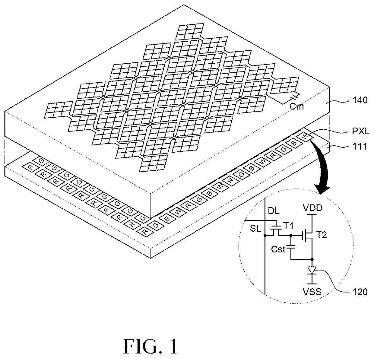
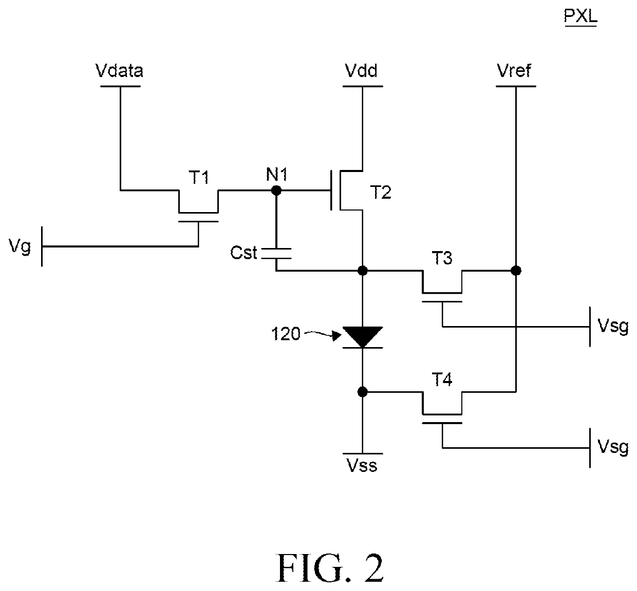
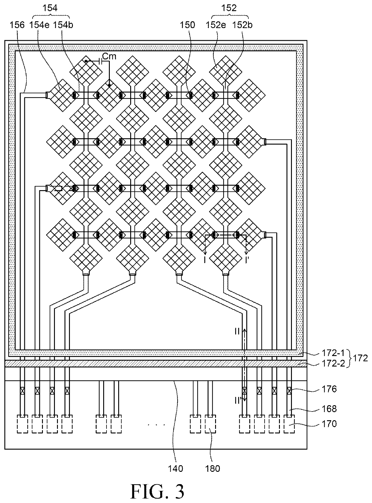
[0020]FIG. 1 is an exploded perspective view of an organic light emitting display device in which a touch sensor is integrated. FIG. 2 is a circuit diagram of a sub-pixel illustrated in FIG. 1. FIG. 3 is a plan view of the organic light emitting display device illustrated in FIG. 1. FIG. 4 is a cross-sectional view of the organic light emitting display device taken along line I-I′ in FIG. 3.

[0021]The organic light emitting display device having the touch sensor illustrated in FIG. 1 senses presence or absence of a touch and a touch position by detecting variances in mutual capacitance (Cm; touch sensor) by a user's touch through touch electrodes 152e and 154e illustrated in FIG. 2 during a touch period. In addition, the organic light emitting display device having the touch sensor illustrated in FIG. 1 displays an image through a unit pixel including a light emitting element 120. The unit pixel is composed of sub-pixels PXL of red (R), green (G) and blue (B), or composed of sub-pixe...


PUM


Abstract

A light emitting display device includes: a substrate including a display area in which a plurality of display pixels are disposed and a non-display area surrounding the display area; an encapsulation film covering the display area and the non-display area and having a first inorganic encapsulation layer, an organic encapsulation layer, and a second inorganic encapsulation layer stacked in an order; a first touch electrode disposed on the encapsulation film and extending in a first direction and a second touch electrode extending in a second direction; at least one inorganic insulating layer disposed on the substrate; a first planarization layer disposed on the inorganic insulating layer; a second planarization layer disposed on the first planarization layer; and a hole pattern formed in the second planarization layer. The hole pattern has the organic encapsulation layer therein.

Description

CROSS-REFERENCE TO RELATED APPLICATIONS[0001]This application claims the benefit of and priority to Korean Patent Application No. 10-2020-0172096 filed on Dec. 10, 2020 in the Republic of Korea, the entire contents of which are hereby expressly incorporated by reference into the present application.BACKGROUNDTechnical Field[0002]The present disclosure relates to a light emitting display device with an integrated touch screen and a method of manufacturing the same, and more particularly, to a light emitting display device with an integrated touch screen that has improved durability and a method of manufacturing the same.Description of the Related Art[0003]In accordance with development of information technology, markets for display devices, which are connection mediums between users and information, are growing. Accordingly, the use of display devices such as organic light emitting displays (OLEDs) and liquid crystal displays (LCDs) is increasing.[0004]The display device includes a d...

Claims


Application Information

Patent Timeline
IPC IPC(8): G06F3/041H01L27/32H01L51/52H01L51/56G06F3/044
CPCG06F3/0412H01L27/323H01L27/3244H01L51/5253H01L51/56G06F2203/04102G06F3/04164H01L2227/323G06F2203/04103G06F2203/04111G06F3/0446G06F3/041662G06F3/0445H10K59/40H10K59/124H10K59/131H10K59/1201H10K71/00H10K59/873G06F2203/04112H10K50/844H10K59/12
Inventor JANG, GEONHA, JONGMOO
Owner LG DISPLAY CO LTD
Why Eureka
Try Eureka