Method of fabricating a conductive layer on an IC using non-lithographic fabrication techniques

a fabrication technique and conductive layer technology, applied in the direction of semiconductor devices, semiconductor/solid-state device details, printed circuits, etc., can solve the problem of significant impact on total production costs

Pending Publication Date: 2022-07-21
PRAGMATIC PRINTING
View PDF0 Cites 2 Cited by
  • Summary
  • Abstract
  • Description
  • Claims
  • Application Information

AI Technical Summary

Problems solved by technology

Due to the large volume of ICs, even relatively small reductions in the complexity and/or cost of flexi...

Method used


Image

  • Method of fabricating a conductive layer on an IC using non-lithographic fabrication techniques
  • Method of fabricating a conductive layer on an IC using non-lithographic fabrication techniques
  • Method of fabricating a conductive layer on an IC using non-lithographic fabrication techniques

Examples


Embodiment Construction

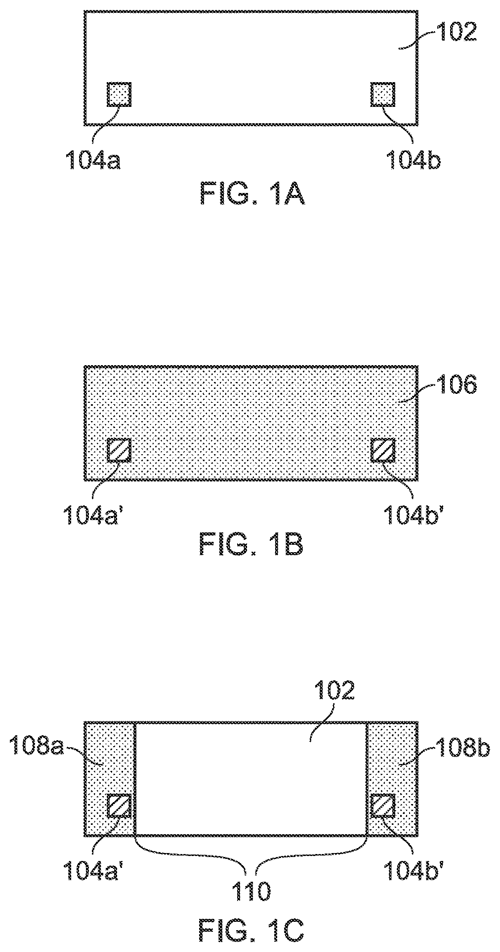
[0031]The fabrication of thin-film ICs, such as flexible ICs for instance, commonly involves the deposition of a material onto a flexible substrate or a previously fabricated layer and the subsequent patterning of the material. This process may then be repeated a number of times to form a plurality of layers of patterned materials that form the electronic components of the thin-film IC.

[0032]The deposition of the materials may be performed using a number of different approaches, such as physical or chemical deposition, which themselves include many different techniques including evaporation techniques, sputtering techniques, plating techniques, printing-based techniques and chemical vapour deposition for example, where these techniques are often used to deposit a blanket layer of material onto a substrate or previously patterned material / layer.

[0033]Following the deposition of a layer of material, selected parts of the material may be removed during a patterning process in order to ...


PUM


Abstract

A method for fabricating a thin-film integrated circuit, IC, including a plurality of electronic components, the method comprising: forming, using a first fabrication technique, the plurality of electronic components, and forming, using a second fabrication technique, a conductive layer on the plurality of electronic components to form a redistribution layer, RDL, wherein the first fabrication technique includes photolithographic patterning, and the first fabrication technique is different to the second fabrication technique.

Description

FIELD OF THE DISCLOSURE[0001]The present disclosure relates to methods for non-lithographic patterning, and in particular, the use of non-lithographic patterning in the manufacture of thin-film integrated circuits.BACKGROUND OF THE DISCLOSURE[0002]Thin-film or flexible Integrated circuits (ICs) are often used in scenarios where large volumes of ICs are required at a relatively low cost. For example, flexible ICs may be used in large numbers for asset tracking or environmental monitoring. Due to the large volume of ICs, even relatively small reductions in the complexity and / or cost of flexible ICs themselves and / or their manufacturing process can have significant impacts on total production costs.[0003]Consequently, there is need for approaches for reducing the complexity and / or cost of flexible ICs and their manufacturing process.BRIEF SUMMARY OF THE DISCLOSURE[0004]It is an aim of certain examples of the present disclosure to provide a reduced complexity and / or duration manufacturi...

Claims


Application Information

Patent Timeline
IPC IPC(8): H01L23/00H01L23/498H01L23/522
CPCH01L24/19H01L24/20H01L23/4985H01L23/562H01L2924/3511H01L24/05H01L24/82H01L2924/3512H01L23/5225H01L2224/02317H01L2224/02311H01L2224/02372H01L2224/03318H01L2224/05548H01L2224/04105H01L2924/3025H01L2223/6677H01L2924/19042H01L2924/19104H01L2224/83203H01L2224/83851H01L2224/2919H01L2224/83101H01L2224/81192H01L2224/81191H01L2224/81193H01L2224/81903H01L2224/81898H01L24/02H01L24/13H01L24/81H01L24/83H01L24/16H01L2224/32145H01L2224/32225H01L2224/32265H01L2224/16145H01L2224/16238H01L2224/16265H01L23/552H01L23/645H01L2924/00015H01L2924/00014H05K1/181H05K1/188H01L23/367H01L24/32H01L2224/16268H01L2224/32268H01L2224/81203H01L2924/30105
Inventor WILLIAMSON, KENPRICE, RICHARD
Owner PRAGMATIC PRINTING
Why Eureka
Try Eureka