Display device

a display device and display device technology, applied in semiconductor devices, semiconductor/solid-state device details, instruments, etc., can solve the problem of limiting the implementation of an extreme narrow bezel, and achieve the effect of maximizing the display area, minimizing the bezel area, and improving the aesthetic sense of the display devi

Pending Publication Date: 2022-09-29
LG ELECTRONICS INC
View PDF0 Cites 2 Cited by
  • Summary
  • Abstract
  • Description
  • Claims
  • Application Information

AI Technical Summary

Benefits of technology

[0024]Effects of a display device according to the present disclosure will be described below.
[0025]According to the present disclosure, a display device capable of maximizing a display area and minimizing a bezel area. As a result, according to the present disclosure, there is an advantage in that an aesthetic sense of the display device can be improved and an image immersion sense of a user can be significantly improved.

Problems solved by technology

However, there is a limit to implement an extreme narrow bezel through simple arrangement change of the pads and the driving elements, so other methods need to be devised.

Method used


Image

  • Display device
  • Display device
  • Display device

Examples


Embodiment Construction

[0038]Hereinafter, preferred embodiments of the present disclosure will be described with reference to the accompanying drawings. Throughout the present disclosure, like reference numerals mean substantially like elements. In the following description, a detailed explanation of known technologies or configurations related to the present disclosure may be omitted to avoid unnecessarily obscuring the subject matter of the present disclosure. In describing various embodiments, like elements may be omitted in another embodiment in which the elements are representatively described at a beginning part.

[0039]Terms including an ordinary number, such as first and second, are used for describing various elements, but the elements are not limited by the terms. The terms are used only to discriminate one element from another element.

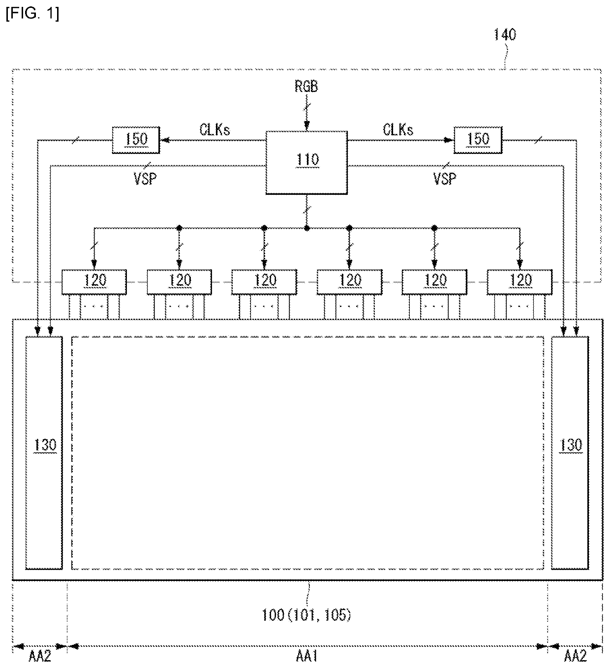
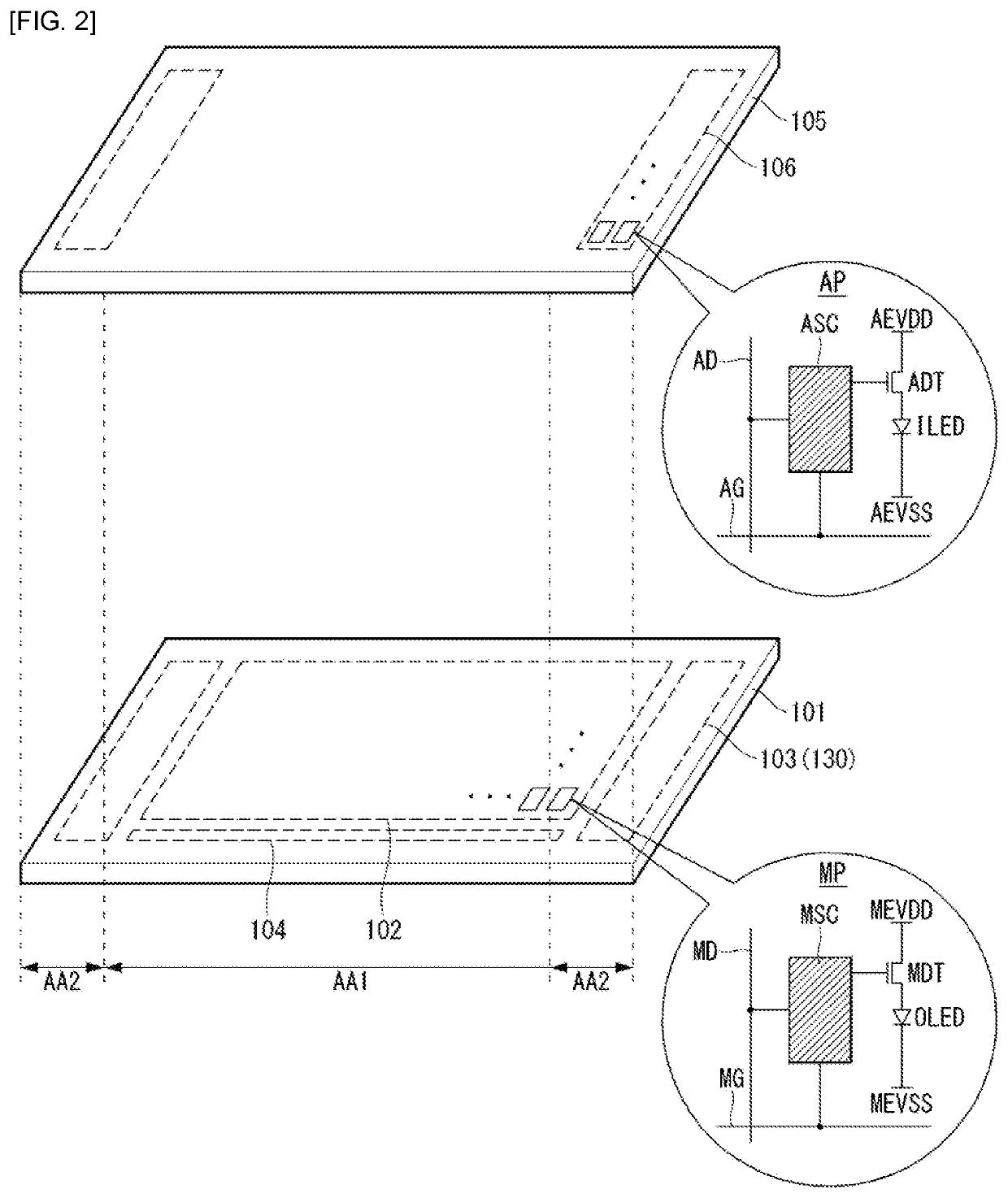
[0040]FIG. 1 is a diagram schematically illustrating a display device according to the present disclosure. FIG. 2 is a perspective view schematically illustrating a...


PUM


Abstract

A display device is disclosed. According to one aspect of the present invention, provided is a display device comprising a display panel having a first display area and a second display area on the outside of the first display area, wherein the display panel comprises: a first substrate which includes a main pixel unit disposed in the first display area and having main pixels, and a GIP unit disposed in the second display area and generating a gate signal; and a second substrate which is bonded to the first substrate and includes an auxiliary pixel unit disposed in the second display area and having auxiliary pixels, the GIP unit supplying the gate signal to the main pixels and the auxiliary pixels.

Description

TECHNICAL FIELD[0001]The present disclosure relates to a wireless communication system and, more particularly, to a method of transmitting a V2X message and an apparatus supporting the same.BACKGROUND ART[0002]Various display apparatuses have been developed, which can reduce a weight and a volume as disadvantages of a cathode ray tube. Such display apparatuses can be implemented by a liquid crystal display (LCD), a field emission display (FED), a plasma display panel (PDP), a quantum dot display (QD), and an electroluminescence display.[0003]A display panel constituting the display apparatus includes a display area in which pixels are arranged to implement an input image, and a non-display area on the outside of the display area. The non-display area may be referred to as a bezel area. The pixels may be defined by an intersection structure of signal lines. The signal lines may include gate lines, data lines, and power lines.[0004]The pixels may include a light emitting element drive...

Claims


Application Information

Patent Timeline
Patent Type & Authority Applications(United States)
IPC IPC(8): H01L25/16H01L27/32H01L25/18H01L23/00
CPCH01L25/167H01L27/3276H01L25/18H01L24/05H01L24/08H01L24/02H01L2224/02145H01L2224/02381H01L2224/05548H01L2224/05558H01L2224/05573H01L2224/08146G09G3/3266H01L25/0753H10K59/00H10K59/131H01L27/156H10K59/12H10K50/00G09G3/32G09G3/3233G09G2300/0426G09G2310/0286H01L2224/08145
Inventor KIM, TAEHOONKIM, SANGYEOLHAM, DONGHO
Owner LG ELECTRONICS INC
Why Eureka
Try Eureka