Check patentability & draft patents in minutes with Patsnap Eureka AI!

Semiconductor memory device, electronic system including the same, and method of fabricating the same

a memory device and semiconductor technology, applied in semiconductor devices, semiconductor/solid-state device details, electrical apparatus, etc., to achieve the effect of improving product reliability and improving process margins

Pending Publication Date: 2022-11-10
SAMSUNG ELECTRONICS CO LTD
View PDF6 Cites 0 Cited by
  • Summary
  • Abstract
  • Description
  • Claims
  • Application Information

AI Technical Summary

Benefits of technology

[0005]Embodiments of the present disclosure provide a semiconductor memory

Problems solved by technology

However, as expensive equipment is required for the miniaturization of patterns, there stil

Method used


Image

  • Semiconductor memory device, electronic system including the same, and method of fabricating the same
  • Semiconductor memory device, electronic system including the same, and method of fabricating the same
  • Semiconductor memory device, electronic system including the same, and method of fabricating the same

Examples


Embodiment Construction

[0031]Semiconductor memory devices according to embodiments of the present disclosure will hereinafter be described with reference to FIG. 1 through FIG. 14.

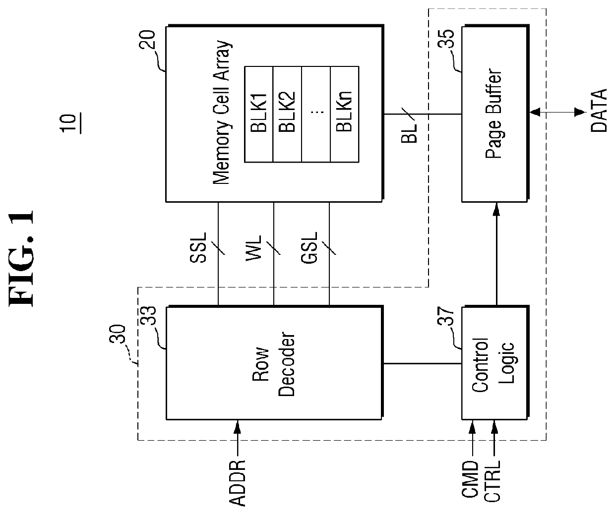
[0032]FIG. 1 is a block diagram illustrating a semiconductor memory device according to some embodiments of the present disclosure.

[0033]Referring to FIG. 1, a semiconductor memory device 10 includes a memory cell array 20 and a peripheral circuit 30.

[0034]The memory cell array 20 may include a plurality of memory cell blocks including a first memory cell block BLK1 through n-th memory cell block BLKn. Each of the first memory cell block BLK1 through n-th memory cell block BLKn may include a plurality of memory cells. The memory cell array 20 may be connected to the peripheral circuit 30 through bitlines BL, wordlines WL, one or more string selection lines SSL, and one or more ground selection lines GSL. Specifically, the first memory cell block BLK1 through n-th memory cell block BLKn may be connected to a row decoder 33 throug...


PUM


Abstract

A semiconductor memory device includes a mold structure including a plurality of wordlines on a front side of a first substrate, and a string selection line and a stopper line on the plurality of wordlines. A channel structure extends in a vertical direction to penetrate the mold structure. A block separation area extends in a first direction to cut the mold structure. A protective structure is interposed between the block separation area and the stopper line and not between the block separation area and the string selection line and not between the block separation area and the plurality of wordlines. A string separation structure extends in the first direction to cut the string selection line and the stopper line. A bitline extends in a second direction on the mold structure. A bitline contact connects the channel structure and the bitline.

Description

CROSS-REFERENCE TO RELATED APPLICATION[0001]This U.S. non-provisional patent application claims the benefit of priority under 35 U.S.C. § 119 to Korean Patent Application No. 10-2021-0058470, filed on May 6, 2021 in the Korean Intellectual Property Office, the disclosure of which is incorporated herein by reference in its entirety.BACKGROUND1. Technical Field[0002]The present disclosure relates to a semiconductor memory device, an electronic system including the same, and a method of fabricating the same. More particularly, the present disclosure relates to a semiconductor memory device including bitline contacts, an electronic is system including the semiconductor memory device, and a method of fabricating the semiconductor memory device.2. Description of the Related Art[0003]There has been a demand for raising the integration density of semiconductor memory devices in order to meet customer demands for high performance and low price. For example, integration density is one of the ...

Claims


Application Information

Patent Timeline
IPC IPC(8): H01L27/11575H01L23/522H01L27/11582H01L27/11573
CPCH01L27/11575H01L23/5226H01L27/11582H01L27/11573H10B43/50H10B43/40H10B43/27H01L25/0657H01L2225/06541H10B43/10H10B43/20H10B43/30
Inventor RYU, HYO JOONKIM, HEE SUKSUNG, JEONG YONGHAN, JEE HOON
Owner SAMSUNG ELECTRONICS CO LTD
Features
  • R&D
  • Intellectual Property
  • Life Sciences
  • Materials
  • Tech Scout
  • Unparalleled Data Quality
  • Higher Quality Content
  • 60% Fewer Hallucinations
Learn More