Memory with memory cells that include a MIM type capacitor with a lower electrode made for reduced resistance at an interface with a metal film

a memory cell and capacitor technology, applied in the field of semiconductor devices, can solve the problems of increasing the leak current of the capacitor, and increasing the thickness of the film on the side wall and the bottom portion, so as to reduce the process margin for layer alignment, small leak current, and the effect of not increasing the number of fabrication processes

Inactive Publication Date: 2007-06-28
ELPIDA MEMORY INC
View PDF10 Cites 18 Cited by
  • Summary
  • Abstract
  • Description
  • Claims
  • Application Information

AI Technical Summary

Benefits of technology

[0016] It is therefore an object of the present invention to provide an MIM type capacitor in which a lower electrode is made thick only at its bottom portion and which is capable of reducing the number of fabrication processes and securing the alignment margin, and a fabrication method for the capacitor.
[0018] It is a further object of the invention to provide an MIM type capacitor which reduces the resistance at the interface between its lower electrode and barrier metal film by increasing the process margin for layer alignment, and a fabrication method for the capacitor.
[0036] The invention provides an MIM type capacitor whose lower electrode is made thick only at its bottom portion without increasing the number of fabrication processes and reducing the process margin for layer alignment. The interface between the lower electrode and barrier metal film of the acquired MIM type capacitor is not oxidized and the capacitor has a small leak current and a low conductive resistance.
[0037] The invention is further characterized in the structure where a second barrier metal film of the same material as the first barrier metal film is laminated on the bottom portion of the lower electrode. The invention can therefore reduce the resistance at the interface between the lower electrode and barrier metal film by increasing the process margin for layer alignment.

Problems solved by technology

As the micropatterning of memory cells becomes finer with the advancement of the microfabrication technology, the amount of electric charges stored in a capacitor undesirably becomes smaller.
Further, the volume expansion that also occurs due to the formation of the titanium oxide film brings about a problem of applying stress to the capacitor, thereby increasing the leak current of the capacitor.
However, increasing the thickness of the lower electrode by CVD normally causes a film of the same thickness to grow on the side wall portion and the bottom portion.
However, the prior art illustrated in FIG. 4 has a problem that forming only the bottom portion of the hole in a step separate from the formation of the capacitor portion increases the number of required steps.

Method used


Image

  • Memory with memory cells that include a MIM type capacitor with a lower electrode made for reduced resistance at an interface with a metal film
  • Memory with memory cells that include a MIM type capacitor with a lower electrode made for reduced resistance at an interface with a metal film
  • Memory with memory cells that include a MIM type capacitor with a lower electrode made for reduced resistance at an interface with a metal film

Examples


first embodiment

[0086] (1) Structure

[0087]FIG. 5 is a longitudinal cross-sectional view showing illustrating a capacitor according to the first embodiment of the present invention.

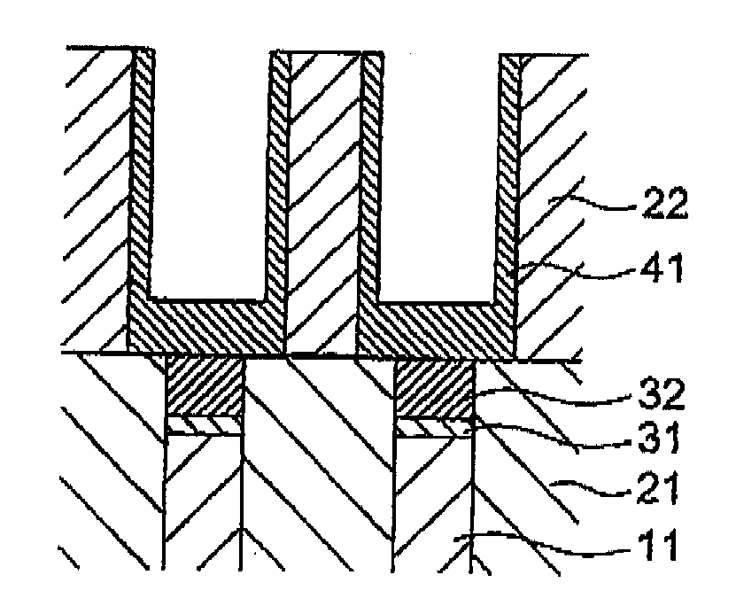
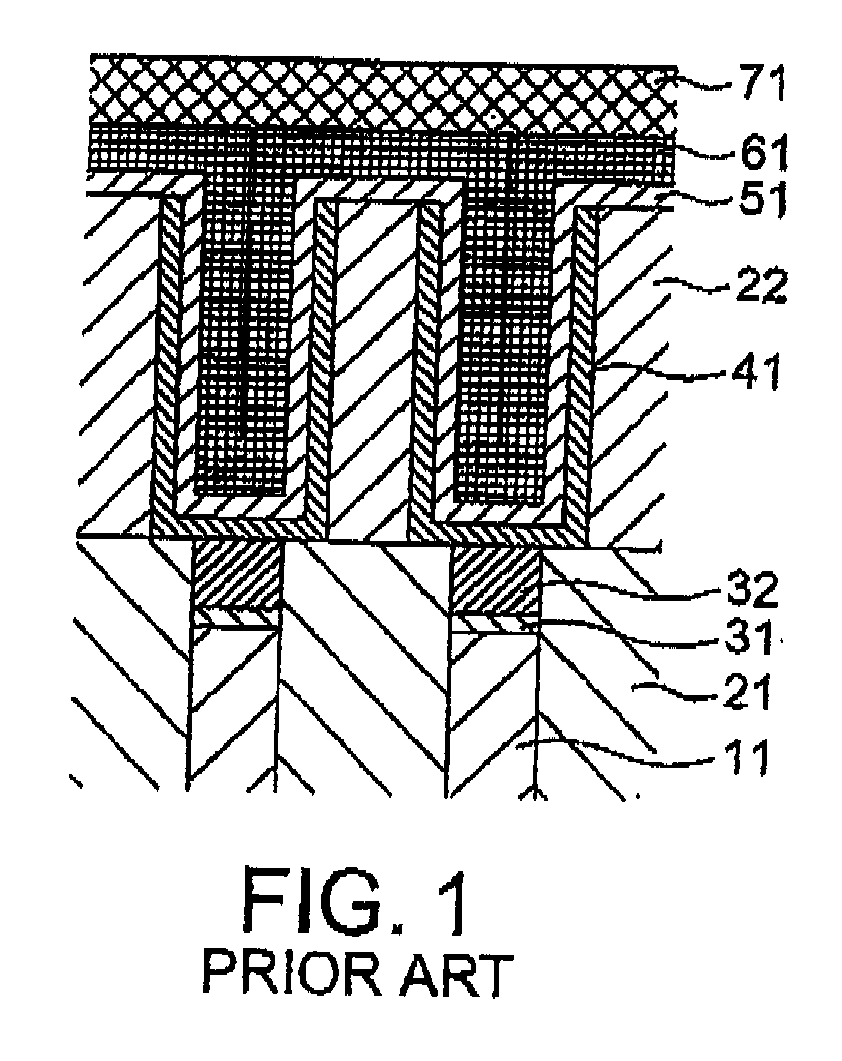
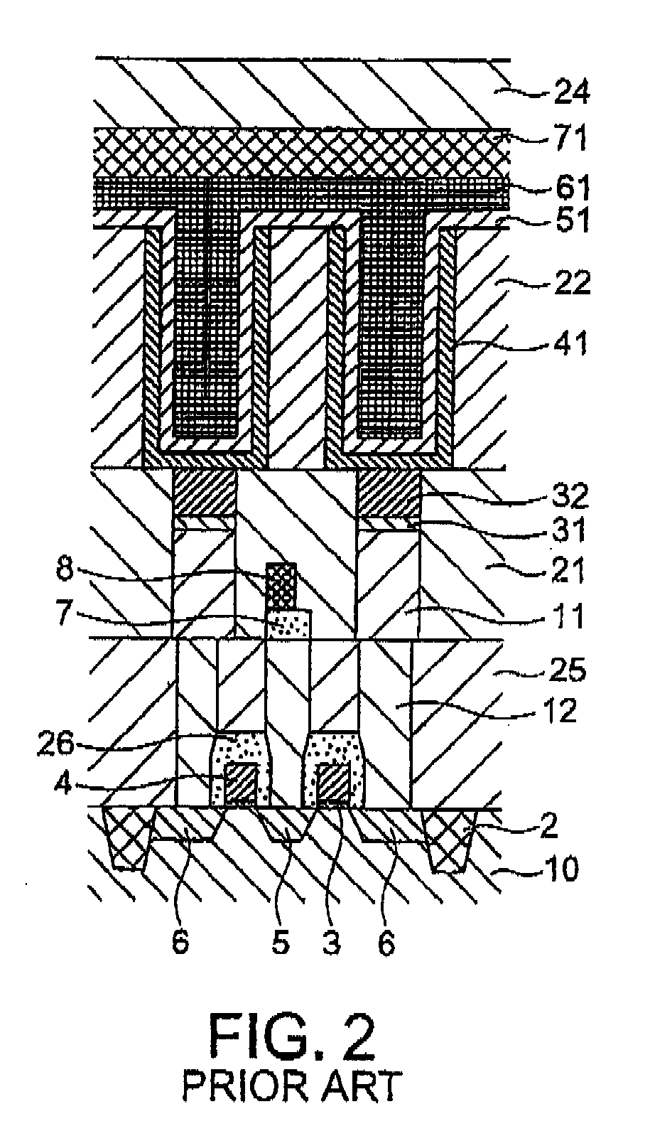
[0088] The capacitor according to the embodiment is formed on an interlayer insulating film 21 which covers an underlying device. The capacitor is constructed by laminating a ruthenium film 41 as a lower electrode, a ruthenium film 61 as an upper electrode and a tantalum oxide film 51 as a capacitive insulating film in a hole provided in an interlayer insulating film 22 formed on the interlayer insulating film 21.

[0089] The lower electrode 41 is connected at its bottom to a barrier metal film 32 which is connected at its bottom surface to a polysilicon plug 11 via a contact metal film 31. The polysilicon plug 11 is further connected to a diffusion layer region (equivalent to “6” in FIG. 2) via an underlying polysilicon plug (equivalent to “12” in FIG. 2).

[0090] In the embodiment, as the bottom portion of the lower ele...

second embodiment

[0126] (1) Structure

[0127]FIG. 25 is a longitudinal cross-sectional view showing illustrating a capacitor according to the second embodiment of the present invention. The second embodiment is an application example in which a metal plug 35 is used in place of the polysilicon plug and barrier metal film in the first embodiment (FIG. 5).

[0128] The lower electrode 41 of the capacitor according to the second embodiment is connected at its bottom to the metal plug 35 which comprises a tungsten film 37 and a titanium nitride film 36. The metal plug 35 is connected to a diffusion layer region (equivalent to “6” in FIG. 2) via an underlying polysilicon plug (equivalent to “12” in FIG. 2).

[0129] As the bottom portion of the lower electrode 41 is thick, the diffusion of oxygen is sufficiently restrained, so that even when a tungsten film which is inferior in oxidation resistance to a titanium nitride film is connected directly to the lower electrode 41, there does not arise a problem that ...

third embodiment

[0135] (1) Structure

[0136]FIG. 29 is a longitudinal cross-sectional view showing illustrating a capacitor according to the third embodiment of the present invention. The third embodiment is an application example in which a titanium nitride film is used for the lower electrode and the upper electrode of the in the second embodiment (FIG. 25) in place of the ruthenium film.

[0137] The capacitor according to the embodiment is formed on the interlayer insulating film 21 which covers an underlying device. The capacitor is constructed by laminating a titanium nitride film 46 as the lower electrode, a titanium nitride film 66 as the upper electrode and the tantalum oxide film 51 as the capacitive insulating film in a hole provided in the interlayer insulating film 22 formed on the interlayer insulating film 21.

[0138] The lower electrode 46 of the capacitor is connected at its bottom to the metal plug 35 which comprises the tungsten film 37 and the titanium nitride film 36. The metal plu...


PUM


Abstract

A semiconductor device includes memory cells each having an MISFET for memory selection formed on one major surface of a semiconductor substrate and a capacitive element comprised of a lower electrode electrically connected at a bottom portion to one of a source and drain of the MISFET for memory selection via a first metal layer and an upper electrode formed on the lower electrode via a capacitive insulating film. The lower electrode has a thickness of 30 nm or greater at the bottom portion thereof. Sputtering with a high ionization ratio and high directivity, such as PCM, is adapted to the formation of the lower electrode to make only the bottom portion of a capacitor thicker.

Description

[0001] This is a divisional of application Ser. No. 10 / 777,704 filed Feb. 13, 2004. [0002] The entire disclosure of the prior application, application Ser. No. 10 / 777,704 is hereby incorporated by reference. [0003] This application claims priority to prior application JP 2003-36459, the disclosure of which is incorporated herein by reference.BACKGROUND OF THE INVENTION [0004] (1) Field of the Invention [0005] The present invention relates to a semiconductor device and a fabrication method therefor, and, more particularly, to an MIM (Metal Insulator Metal) type capacitor and a fabrication method therefor. [0006] (2) Description of the Related Art [0007] Each of memory cells of a DRAM (Dynamic Random Access Memory) comprises a selection transistor and a capacitor. As the micropatterning of memory cells becomes finer with the advancement of the microfabrication technology, the amount of electric charges stored in a capacitor undesirably becomes smaller. To solve this problem, active st...

Claims


Application Information

Patent Timeline
Patent Type & Authority Applications(United States)
IPC IPC(8): H01L21/20H01L21/02H01L21/8242H01L21/768H01L27/108H01L29/76
CPCH01L21/7687H01L27/10814H01L27/10852H01L28/65H10B12/315H10B12/033
Inventor NAKAMURA, YOSHITAKAGOTO, HIDEKAZUASANO, ISAMUHORIKAWA, MITSUHIROKUROKI, KEIJISAKUMA, HIROSHIKOYANAGI, KENICHIKAWAGOE, TSUYOSHI
Owner ELPIDA MEMORY INC
Why Eureka
Try Eureka