
Semiconductor memory device having self-aligned contacts and method of fabricating the same

a memory device and semiconductor technology, applied in the direction of semiconductor devices, electrical devices, transistors, etc., can solve the problems of difficult photolithographic process for forming contact holes in integrated semiconductor devices having multi-layer interconnection structures, and achieve the effect of simplifying the process

Inactive Publication Date: 2005-04-26
SAMSUNG ELECTRONICS CO LTD
View PDF11 Cites 17 Cited by
  • Summary
  • Abstract
  • Description
  • Claims
  • Application Information

AI Technical Summary

Benefits of technology

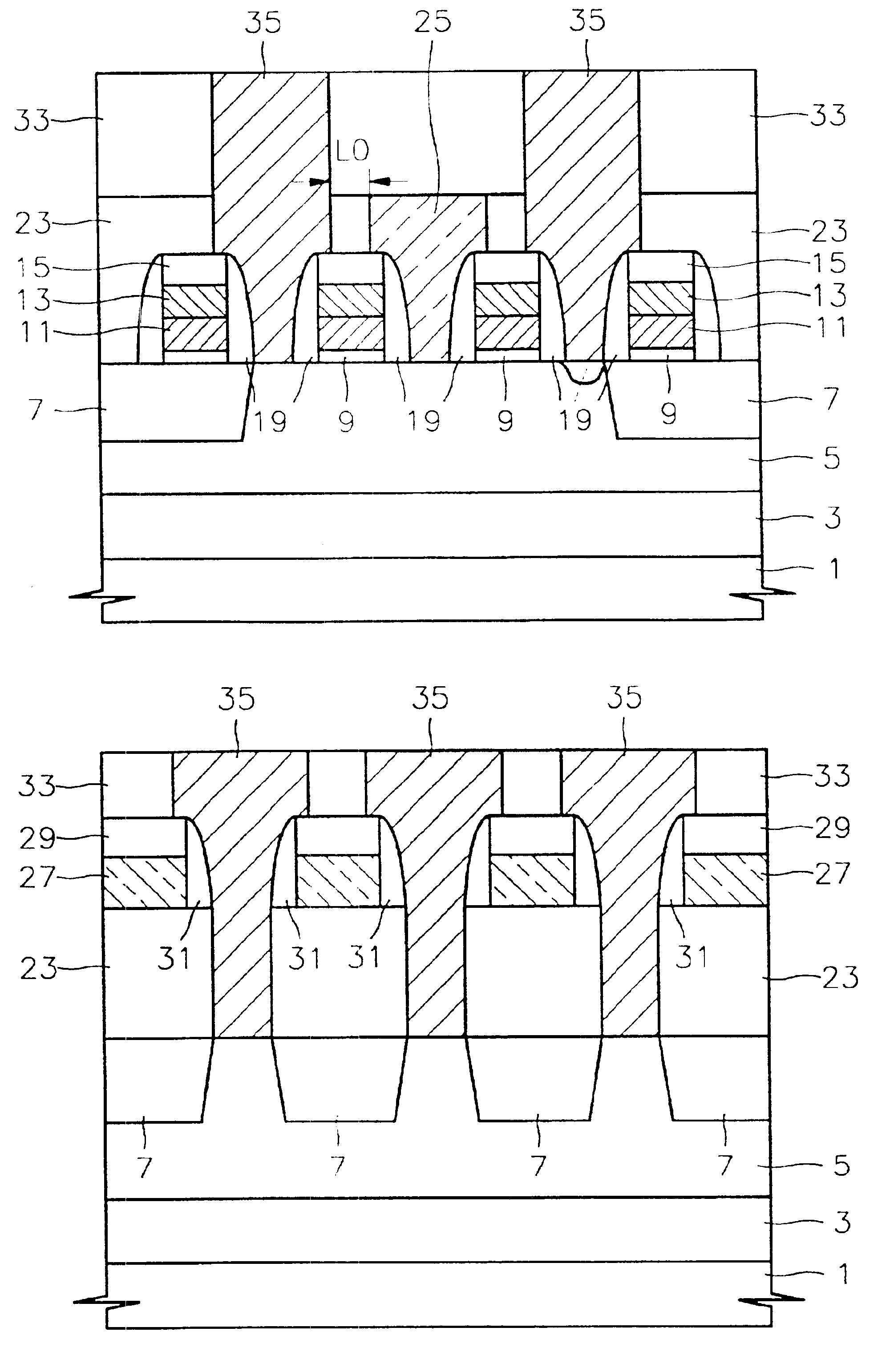
[0010]To solve the above problems, it is an object of the present invention to provide a semiconductor memory device having self-aligned contacts, in which an interval between contacts for bit lines and contacts for storage electrodes is maximized, thereby preventing short-circuit between the contacts for bit lines and the contacts for storage electrodes and increasing a process margin.
[0011]It is another object of the present invention to provide a method of fabricating a semiconductor memory device having self-aligned contacts, in which short-circuit between contacts for bit lines and contacts for storage electrodes is prevented and a process is simplified.
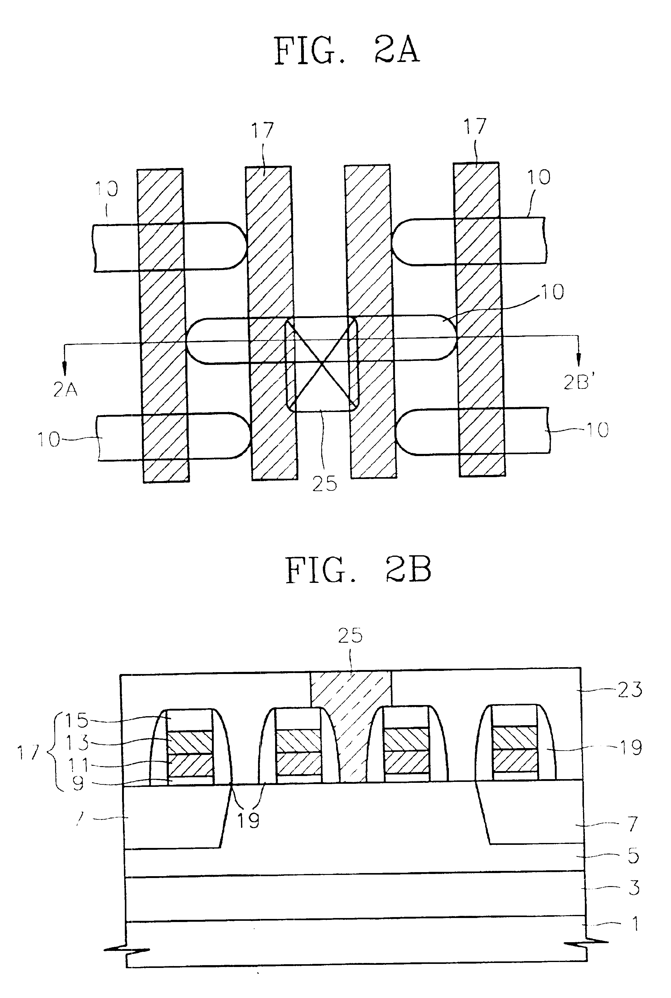
[0024]According to the present invention, since the contacts for storage electrodes are self-aligned with the bit line patterns and the gate electrode patterns, short-circuit between the contacts for bit lines and the contacts for storage electrodes can be prevented. Also, since the height of the surfaces of the contacts for bit lines is formed of the height less than the height of the surfaces of the contacts for gate electrode patterns, a distance between the contacts for bit lines and the contacts for storage electrodes is spaced-apart, and then, short-circuit between the contacts for bit lines and the contacts for storage electrodes can be prevented, and further since the contacts for storage electrodes with respect to the contacts for bit lines can be arranged at a maximum distance, short-circuit between the contacts for bit lines and the contacts for storage electrodes can be prevented, and simultaneously, an adequate process margin for the selection of the position of a contact hole can be obtained.
[0025]In addition, according to the prior art, the contacts for bit lines and the contacts for storage electrodes are formed after pads for bit lines and pads for storage electrodes are formed, however, according to the present invention, the pads are not formed, and thereby, the process is simplified.

Problems solved by technology

Thus, the formation of contact holes using a photolithographic process in integrated semiconductor devices having a multi-layer interconnection structure is more difficult.

Method used


Image

  • Semiconductor memory device having self-aligned contacts and method of fabricating the same
  • Semiconductor memory device having self-aligned contacts and method of fabricating the same
  • Semiconductor memory device having self-aligned contacts and method of fabricating the same

Examples


Embodiment Construction

[0033]The present invention will be described more fully hereinafter with reference to the accompanying drawings in which preferred embodiments of the invention are shown. This invention may, however, be embodied in many different forms and should not be construed as being limited to the embodiments set forth herein. Rather, these embodiments are provided so that this disclosure will be thorough and complete, and will fully convey the scope of the invention to those skilled in the art. In the drawings, the thickness of layers and regions are exaggerated for clarity.

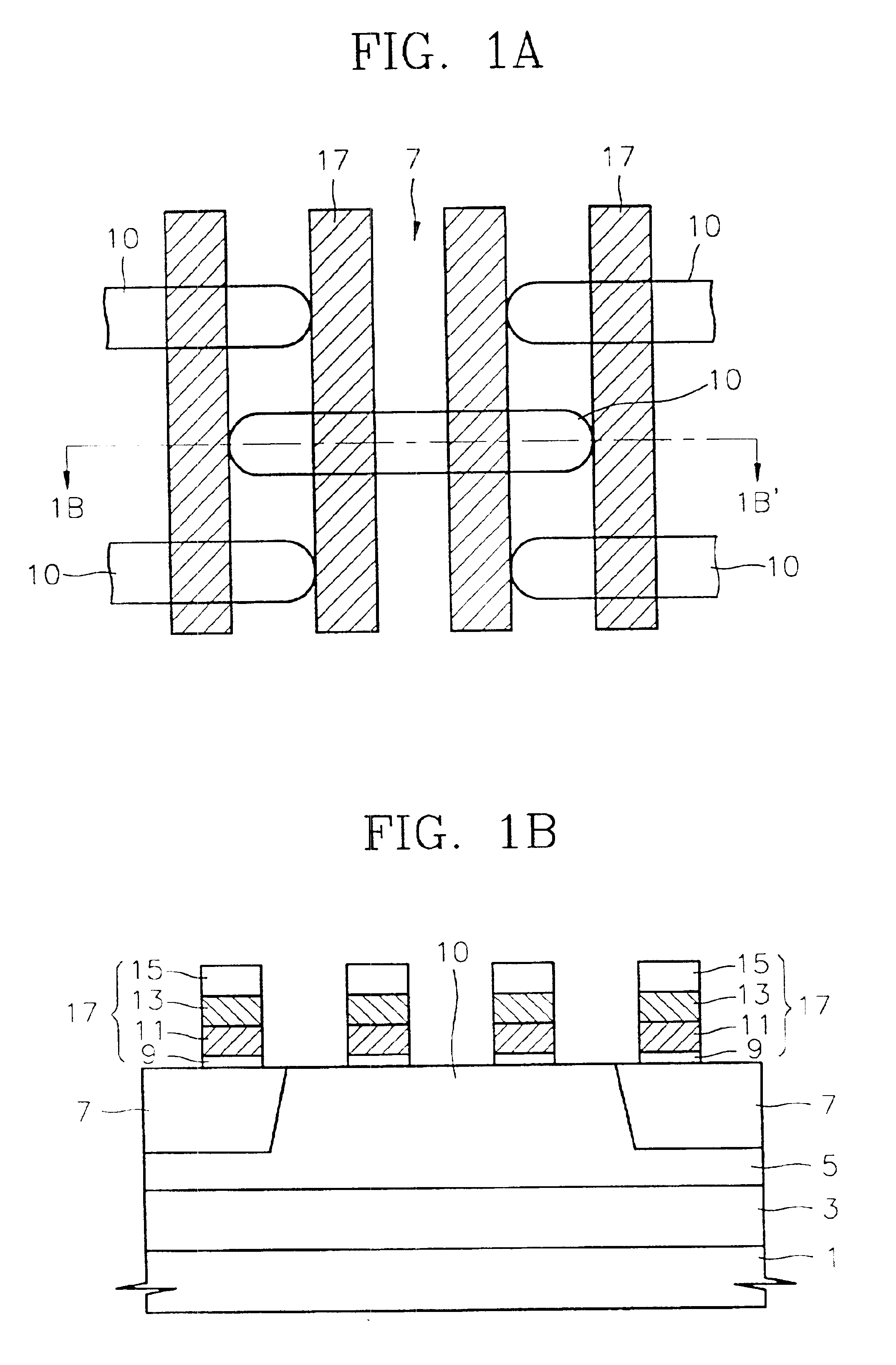
[0034]FIG. 1A is a plan view illustrating steps of forming gate electrode patterns, and FIG. 1B is a sectional view taken along line 1B-1B′ of FIG. 1A.

[0035]Referring to FIGS. 1A and 1B, second conductivity type impurities, for example, an n-type buried impurities layer 3 and a p-type well 5 for forming an NMOS transistor are sequentially formed by a conventional method, for example, by implanting impurity ions around the...


PUM


Abstract

A semiconductor memory device having self-aligned contacts, capable of preventing a short-circuit between contacts for bit lines and contacts for storage electrodes and improving a process margin, and a method of fabricating the same are provided. The semiconductor memory device having self-aligned contacts includes a plurality of gate electrode patterns arranged in parallel on a semiconductor substrate, in which a plurality of first spacers are formed along the sidewalls of the gate electrode patterns, a first interdielectric layer formed on the entire surface of a resultant in which the first spacers are formed, a plurality of bit line patterns arranged in parallel on the first interdielectric layer to be perpendicular to the gate electrode patterns, in which a plurality of second spacers are formed along the sidewalls of the bit line patterns, a plurality of contacts for bit lines self-aligned with the first spacers, a second interdielectric layer formed on the entire surface of a resultant in which the second spacers are formed, and a plurality of contacts for storage electrodes simultaneously self-aligned with the second and first spacers.

Description

BACKGROUND OF THE INVENTION[0001]1. Field of the Invention[0002]The present invention relates to a semiconductor memory device having self-aligned contacts and a method of fabricating the same, and more particularly, to a semiconductor memory device having contacts for storage electrodes which are simultaneously self-aligned with bit lines and gate electrodes in the structure of a capacitor over bit line (COB) in which a capacitor is formed after the formation of the bit lines, and a method of fabricating the same.[0003]2. Description of the Related Art[0004]As the integration of semiconductor devices increases, the size of a unit cell in a memory cell per unit area is reduced. For example, in the case of a dynamic random access memory (DRAM), the cell size is reduced to less than 1.5 μm2. Reduced cell size can be achieved by decreasing an interval between conductive layers of the cell, and in the case of DRAM, due to high integration, an interval between gate electrodes becomes a m...

Claims


Application Information

Patent Timeline
IPC IPC(8): H01L21/02H01L21/70H01L21/60H01L21/8242H01L27/108H01L27/10
CPCH01L21/76897H01L27/10855H01L27/10814H01L27/10888H10B12/315H10B12/485H10B12/0335H01L27/10
Inventor AHN, TAE-HYUKKIM, MYEONG-CHEOLLEE, JUNG-HYEONNAM, BYEONG-YUNMIN, GYUNG-JIN
Owner SAMSUNG ELECTRONICS CO LTD
Learn More