
Semiconductor device and method of fabricating the same

a technology of semiconductor devices and semiconductors, applied in semiconductor devices, basic electric elements, electrical equipment, etc., can solve the problems of distorted region called “bird beak”, different film thicknesses of gate insulating films, and different levels of silicon nitride films serving as stoppers in the cmp process. achieve the effect of sufficient process margin and high level of planarization

Inactive Publication Date: 2008-12-11
KK TOSHIBA
View PDF4 Cites 1 Cited by
  • Summary
  • Abstract
  • Description
  • Claims
  • Application Information

AI Technical Summary

Benefits of technology

[0008]Therefore, an object of the present invention is to provide a semiconductor device in which the difference in the level of the gate oxide films can be overcome so that a sufficient process margin can be ensured in the CMP process and processing achieving a high level of planarization can be carried out, and a method of fabricating such a semiconductor device.

Problems solved by technology

When the gate insulating films have different film thicknesses in the aforesaid fabrication method, the following defect occurs: when a trench serving as shallow trench isolation (STI) is first formed and subsequently, an insulating film buried in the trench is planarized by a chemical mechanical polishing (CMP) process, the difference in the film thicknesses of gate insulating films results in differences in the level of a silicon nitride film serving as a stopper film in the CMP process.
Furthermore, the level difference easily tends to result in discrepancies such as dishing in the CMP process.
However, the method disclosed in the above-noted U.S. patent has the following disadvantage: an oxide film formed by the selective oxidation, namely, LOCOS, results in formation of a distorted region called “bird beak” formed in a peripheral edge of the oxide film.
Consequently, the distorted region needs to be taken into consideration in the design of the semiconductor device, resulting in constraints to reduction I an area of the semiconductor device.

Method used


Image

  • Semiconductor device and method of fabricating the same
  • Semiconductor device and method of fabricating the same
  • Semiconductor device and method of fabricating the same

Examples


Embodiment Construction

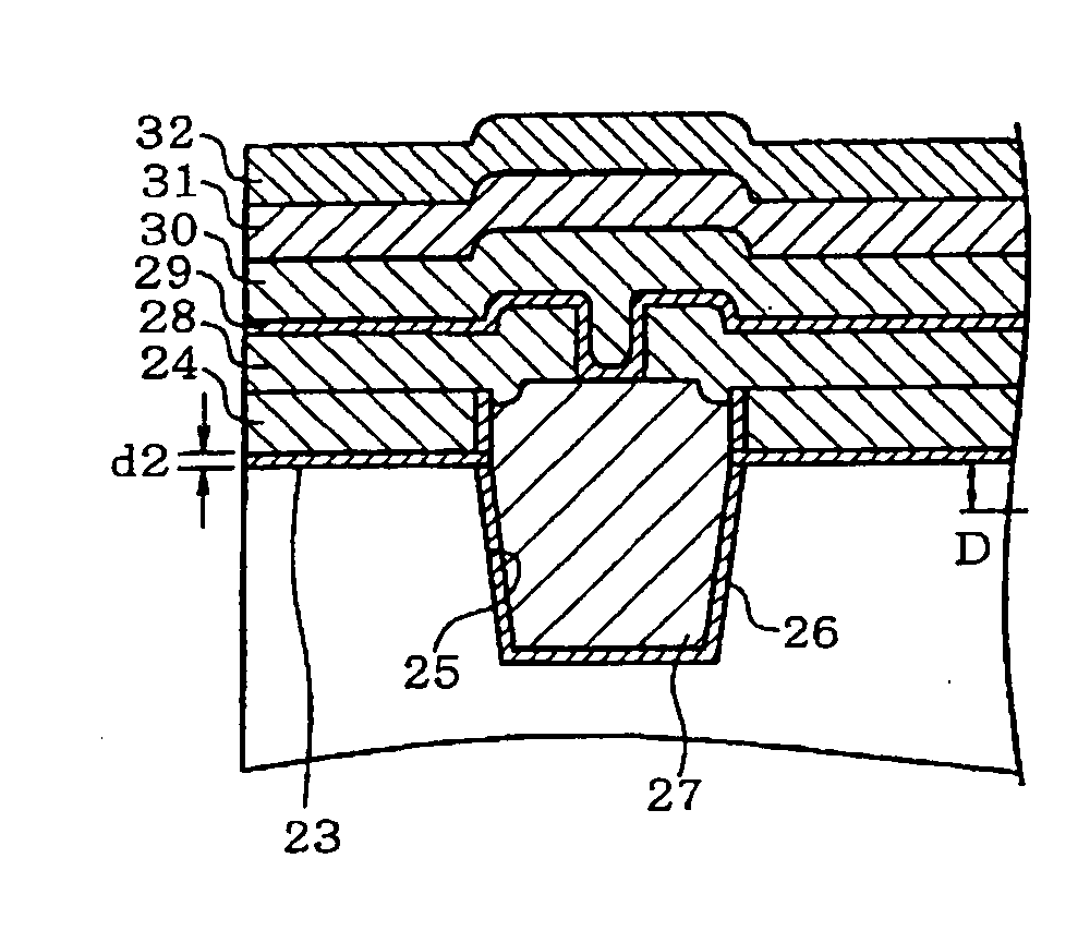
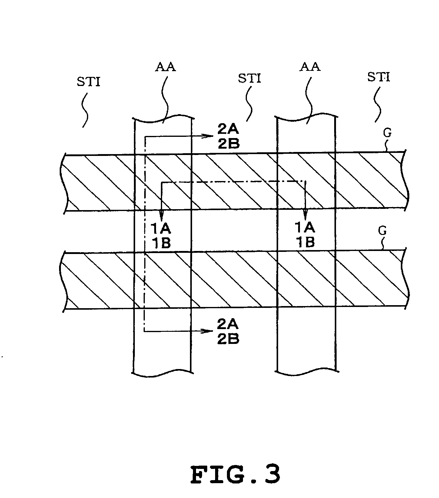
[0020]A first embodiment of the present invention will be described with reference to FIGS. 1A to 5J. The invention is applied to a flash memory in the first embodiment. FIGS. 1A, 1B, 2A and 2B show layer structures of transistors formed in memory cell and peripheral circuit regions respectively. FIG. 3 is a diagrammatic plan view of portions corresponding to FIGS. 1A, 1B, 2A and 2B. FIGS. 1A and 1B are diagrammatic sections taken in the direction traversing an active area AA and shallow trench isolation (STI) on a gate electrode G, namely, along line 1A-1A (1B-1B) in FIG. 3. FIGS. 2A and 2B are diagrammatic sections taken in the direction parallel to the active area AA, namely, along line 2A-2A (2B-2B).

[0021]Referring to FIGS. 1A, 1B, 2A and 2B, a silicon substrate 21 serving as a semiconductor substrate has different thicknesses or a non-uniform thickness. In this case, a part of the substrate corresponding to a high breakdown voltage transistor of the peripheral circuit region ha...


PUM


Abstract

A semiconductor device such as a flash memory includes a semiconductor substrate, two gate insulating films formed on the substrate so as to have a first film thickness and a second film thickness smaller than the first film thickness respectively, and a polycrystalline silicon film formed on the gate insulating films so that parts of the polycrystalline silicon film on the respective gate insulating films are on a level with each other and serving as a gate electrode. The substrate is formed with a recess defined by a bottom and sidewalls substantially perpendicular to the bottom, the recess corresponding to the part of the gate insulating film with the first film thickness.

Description

CROSS-REFERENCE TO RELATED APPLICATIONS[0001]This application is based on and claims the benefit of priority from the prior Japanese Patent Application No. 2004-184948, filed on Jun. 23, 2004, the entire contents of which are incorporated herein by reference.BACKGROUND OF THE INVENTION[0002]1. Field of the Invention[0003]The present invention relates to a semiconductor device including a plurality of gate insulating films with different film thicknesses and a method of fabricating the same.[0004]2. Description of the Related Art[0005]Semiconductor devices of the above-noted type include non-volatile semiconductor devices such as a flash memory. The flash memory comprises a memory cell region and a peripheral circuit region both necessitating different gate breakdown voltages. Accordingly, gate insulating films having different film thicknesses corresponding to the different gate breakdown voltages respectively. In one of methods of fabricating semiconductor devices, a film structure...

Claims


Application Information

Patent Timeline
Patent Type & Authority Applications(United States)
IPC IPC(8): H01L21/76
CPCH01L27/115H01L27/11521H10B69/00H10B41/30
Inventor KAMO, RYUICHIKAJIMOTO, MINORITSUNODA, HIROAKIMURAHAMA, YUUICHIRO
Owner KK TOSHIBA
Learn More