Electrically rewritable non-volatile memory element

a non-volatile, memory element technology, applied in the direction of electrical equipment, semiconductor devices, semiconductor/solid-state device details, etc., can solve the problems of reducing the electrical power consumption of the device, dram is volatile memory that loses stored data, and the limit of the device electrical power consumption can be exceeded, so as to prevent the occurrence of poor connection and reduce the write current. , the effect of high heating efficiency

Active Publication Date: 2009-05-05
MICRON TECH INC
View PDF2 Cites 1 Cited by
  • Summary
  • Abstract
  • Description
  • Claims
  • Application Information

AI Technical Summary

Benefits of technology

[0018]The present invention has been achieved to solve the above problems. It is therefore an object of the present invention to provide a non-volatile semiconductor memory device that includes a recording layer that contains a phase change material, and that can obtain high heating efficiency while sufficiently securing a process margin.
[0026]The non-volatile semiconductor memory device according to the present invention includes a plurality of apertures, arranged in an interlayer insulation film and each having a shape that extends in parallel to each other, so that it becomes possible to form the aperture with higher accuracy as compared to a conventional case in which an independent aperture is formed. Therefore, it is possible to obtain high heating efficiency while effectively preventing occurrence of poor connection or the like.
[0028]When the top surface of the lower electrode has a ring shape, the aperture can be formed at a position for exposing two regions of the top surface of each lower electrode, or at a position for exposing one region of the top surface of each lower electrode. In the former case, the recording layer pattern is preferably formed at a position that contacts only one of the two exposed regions of the lower electrode. On the other hand, in the latter case, the recording layer pattern is preferably formed at a position that contacts only one portion of the exposed regions of the lower electrode. Accordingly, the contact area is further reduced, thereby obtaining higher heating efficiency.
[0035]According to this aspect of the present invention, it is also possible to obtain high heating efficiency while effectively preventing occurrence of poor connection or the like.
[0037]As described above, the non-volatile semiconductor memory device according to the present invention can obtain high heating efficiency while preventing occurrence of poor connection or the like. Therefore, it is possible to reduce a larger amount of write current as compared to the conventional case while securing a sufficient process margin. It is also possible to enhance a writing speed.

Problems solved by technology

DRAM is volatile memory that loses stored data if its power supply is turned off.
That makes DRAM unsuitable for the storage of programs and archival information.
Also, even when the power supply is turned on, the device has to periodically perform refresh operations in order to retain stored data, so there are limits as to how much device electrical power consumption can be reduced, while yet a further problem is the complexity of the controls run under the controller.
Semiconductor flash memory is high capacity and non-volatile, but requires high current for writing and erasing data operations, and these operation times are long.
These drawbacks make flash memory an unsuitable candidate for replacing DRAM in main memory applications.
There are other non-volatile memory devices, such as magnetoresistive random access memory (MRAM) and ferroelectric random access memory (FRAM), but they cannot easily achieve the kind of storage capacities that are possible with DRAM.
This limitation reduces the contact area.
In the non-volatile semiconductor memory device shown in FIG. 12 and FIG. 13, however, one aperture 6a needs be formed for each two lower electrodes 2, which makes it difficult for the aperture 6a to be vertically positioned with the lower electrode.
That is, when an independent aperture 6a having an island-like shape is to be formed, it becomes difficult to correctly control the position of the edge 6b.
As a result, poor connection or the like easily occurs.
In this case, the lower electrode 2 on the left side and the recording layer 8 cannot contact, resulting in poor connection.

Method used


Image

  • Electrically rewritable non-volatile memory element
  • Electrically rewritable non-volatile memory element
  • Electrically rewritable non-volatile memory element

Examples


second embodiment

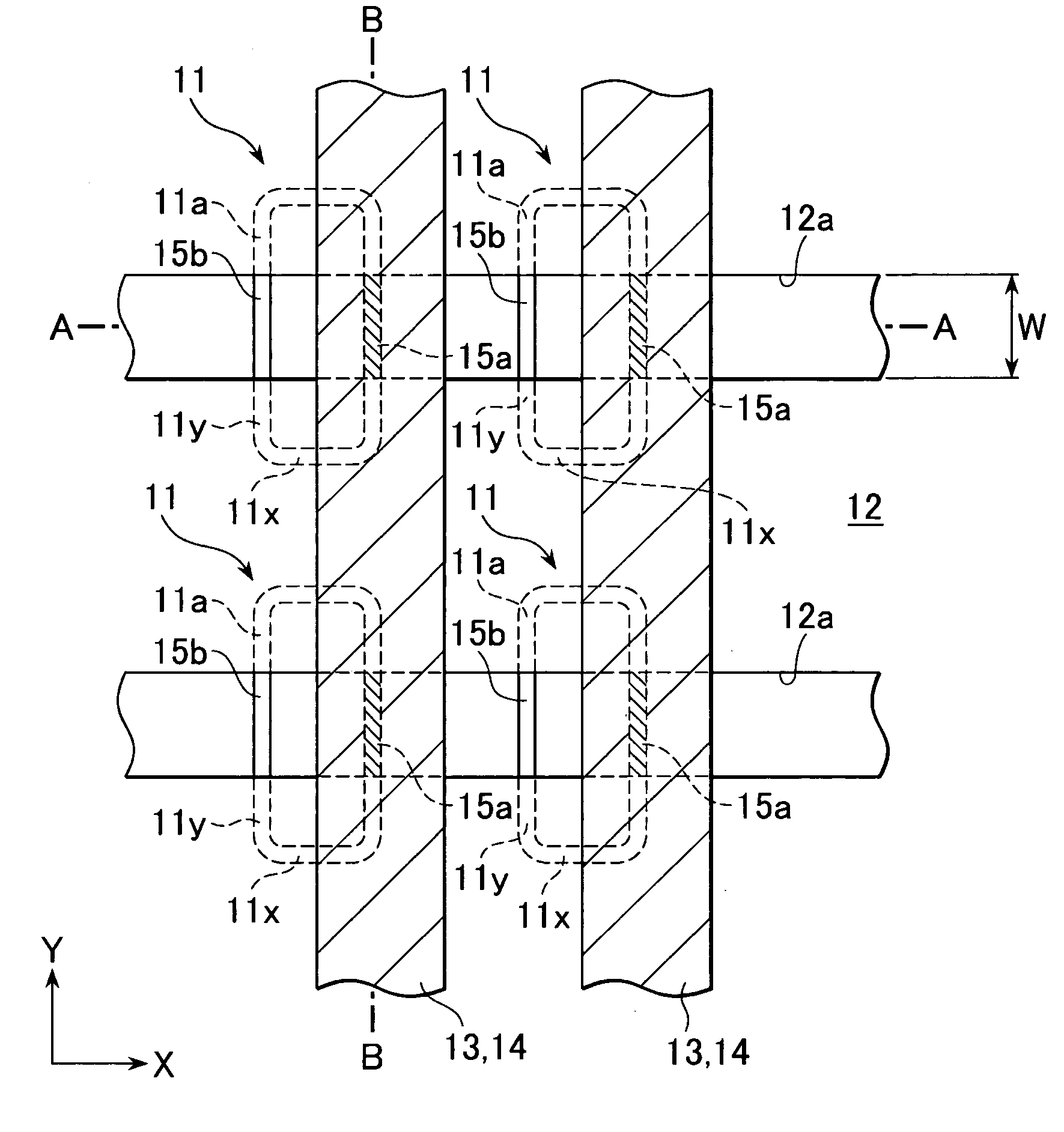
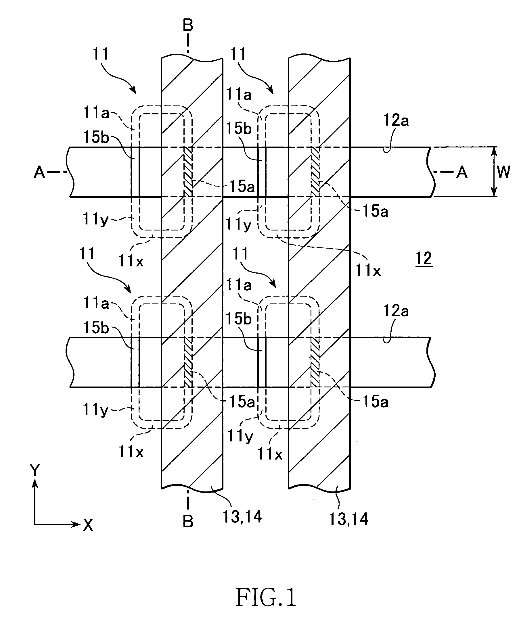
[0092]FIG. 10 is a schematic plan view of the structure of relevant parts of a non-volatile semiconductor memory device according to the present invention.

[0093]As shown in FIG. 10, in the non-volatile semiconductor memory device according to this embodiment, the formation position of the aperture 12a is deviated in the Y direction as compared to the non-volatile semiconductor memory device shown in FIG. 1. Owing to this deviation, each lower electrode 11 exposes the top surface 11a thereof in the entire strip region 11x on one side and in a strip region 11y in the vicinity thereof. That is, in the first embodiment, the aperture 12a is formed at a position where two regions of the top surface 11a of the lower electrode 11 are exposed. On the other hand, in the second embodiment, the aperture 12a is formed at a position where only one region of the top surface 11a of the lower electrode 11 is exposed.

first embodiment

[0094]The formation position of the recording layer 13, however, is set on the strip regionally on one side (right side in FIG. 1), out of the two strip regions 11y of the lower electrode 11, similarly to the Thus, the recording layer 13 contacts only one portion out of exposed regions of the lower electrode 11. That is, the region 15a where the lower electrode 11 and the recording layer 13 contact is further limited to one portion of the top surface 11a of the lower electrode 11 exposed in the aperture 12a.

[0095]With this configuration, in the second embodiment, when the formation position of the aperture 12a in the Y direction or the formation position of the recording layer 13 in the X direction is controlled, it becomes possible to adjust the area of the region 15a. Accordingly, when the formation position of the aperture 12a in the Y direction and the formation position of the recording layer 13 in the X direction are adjusted with high accuracy, it becomes possible to make s...


PUM


Abstract

A non-volatile semiconductor memory device includes a plurality of lower electrodes arranged in a matrix manner, a plurality of recording layer patterns, each being arranged on the lower electrode, that contain a phase change material, and an interlayer insulation film that is provided between the lower electrode and the recording layer pattern and that has a plurality of apertures for exposing one portion of the lower electrode. The lower electrode and the recording layer pattern are connected in each aperture. The apertures extend in the X direction in parallel to one another. The recording layer patterns extend in the Y direction in parallel to one another. Thus the aperture can be formed with higher accuracy as compared to forming an independent aperture. Accordingly, high heating efficiency can be obtained while effectively preventing occurrence of poor connection or the like.

Description

TECHNICAL FIELD[0001]The present invention relates to an electrically rewritable non-volatile memory element. More specifically, the present invention relates to an electrically rewritable non-volatile memory element having a recording layer that includes phase change material.BACKGROUND OF THE INVENTION[0002]Personal computers and servers and the like use a hierarchy of memory devices. There is lower-tier memory, which is inexpensive and provides high storage capacity, while memory higher up the hierarchy provides high-speed operation. The bottom tier generally consists of magnetic storage such as hard disks and magnetic tape. In addition to being non-volatile, magnetic storage is an inexpensive way of storing much larger quantities of information than solid-state devices such as semiconductor memory. However, semiconductor memory is much faster and can access stored data randomly, in contrast to the sequential access operation of magnetic storage devices. For these reasons, magnet...

Claims


Application Information

Patent Timeline
Patent Type & Authority Patents(United States)
IPC IPC(8): H01L47/00
CPCH01L27/2436H01L27/2472H01L45/06H01L45/1233H01L45/126H01L45/143H01L45/144H01L45/148H01L45/1675H10B63/82H10B63/30H10N70/8413H10N70/8825H10N70/231H10N70/884H10N70/8828H10N70/063H10N70/826
Inventor SATO, HOMARENAKAI, KIYOSHI
Owner MICRON TECH INC
Why Eureka
Try Eureka