Organic light-emitting display device

a light-emitting display and organic technology, applied in semiconductor devices, instruments, electrical devices, etc., can solve the problems of reducing production yield and difficulty in realizing high resolution, and achieve the effects of high resolution, high resolution, and sufficient process margin

Active Publication Date: 2020-06-02
LG DISPLAY CO LTD
View PDF9 Cites 1 Cited by
  • Summary
  • Abstract
  • Description
  • Claims
  • Application Information

AI Technical Summary

Benefits of technology

[0009]An aspect of the present disclosure is to provide an organic light-emitting display device that enables the realization of a high resolution.
[0011]To achieve these and other aspects of the inventive concepts, as embodied and broadly described, an organic light-emitting display device comprises a storage capacitor, which overlaps a transistor, with at least one buffer layer interposed therebetween, and which includes a lower storage electrode and an upper storage electrode overlapping the lower storage electrode, with a storage buffer layer interposed therebetween. One of the lower storage electrode and the upper storage electrode is formed to have the same line width and the same shape as the storage buffer layer, thereby ensuring a sufficient process margin and consequently realizing a high resolution and improving production yield.

Problems solved by technology

As such, because the signal lines DL, VL1 and VL2, the transistor area TA and the capacitor area CA are arranged on the substrate to be spaced apart from each other in the horizontal direction, a process margin is small, which makes it difficult to realize a high resolution and reduces production yield.

Method used


Image

  • Organic light-emitting display device
  • Organic light-emitting display device
  • Organic light-emitting display device

Examples


Embodiment Construction

[0022]Reference will now be made in detail to embodiments of the present application, examples of which are illustrated in the accompanying drawings. Wherever possible, the same reference numbers will be used throughout the drawings to refer to the same or like parts.

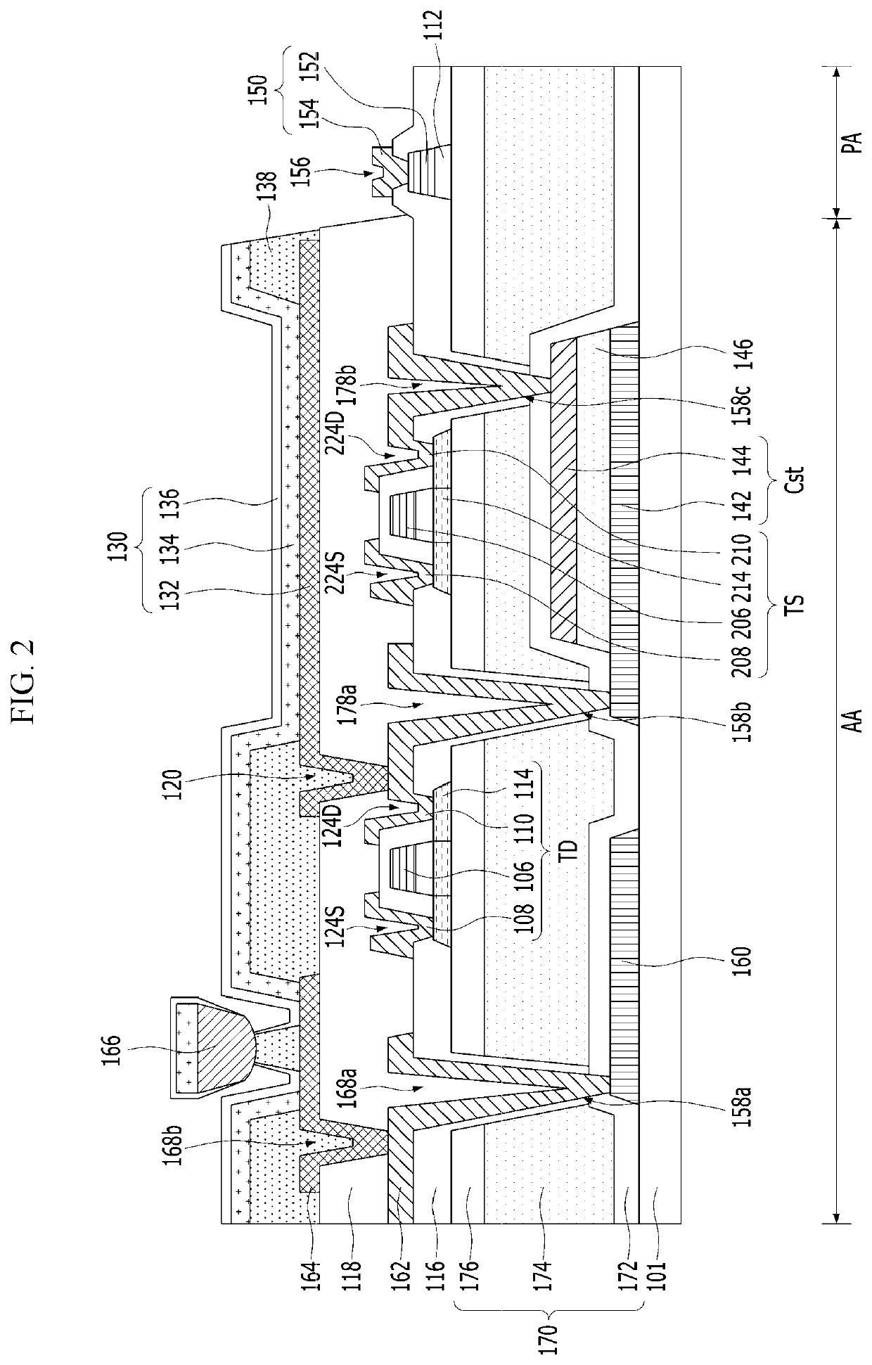
[0023]FIG. 2 is a sectional view of an organic light-emitting display device according to the present invention.

[0024]The organic light-emitting display device shown in FIG. 2 includes an active area AA and a pad area PA.

[0025]A plurality of pads 150 is formed in the pad area PA in order to supply driving signals to a scan line, a data line, a high-voltage VDD supply line and a low-voltage VSS supply line 160, which are disposed in the active area AA.

[0026]Each of the pads 150 includes a pad electrode 152 and a pad cover electrode 154.

[0027]The pad electrode 152 is formed on a gate insulation pattern 112, which has the same shape as the pad electrode 152, using the same material as gate electrodes 206 and 106.

[0028]The ...


PUM

PropertyMeasurementUnit
dielectric constantaaaaaaaaaa
widthaaaaaaaaaa

Abstract

Disclosed is an organic light-emitting display device capable of realizing a high resolution. The organic light-emitting display device includes a storage capacitor disposed on a substrate, which overlaps at least one transistor, with at least one buffer layer interposed therebetween, the at least one buffer layer disposed on the storage capacitor, and which includes a lower storage electrode and an upper storage electrode overlapping the lower storage electrode, with a storage buffer layer interposed therebetween, and a light-emitting diode connected to the transistor. One of the lower storage electrode and the upper storage electrode is formed to have the same line width and the same shape as the storage buffer layer, thereby ensuring a sufficient process margin and consequently realizing a high resolution and improving production yield.

Description

[0001]This application claims the benefit of Korean Patent Application No. 10-2016-0170520, filed on Dec. 14, 2016, which is hereby incorporated by reference as if fully set forth herein.BACKGROUND[0002]Technical Field[0003]The present invention relates to an organic light-emitting display device, and more particularly to an organic light-emitting display device that enables the realization of a high resolution.[0004]Discussion of the Related Art[0005]An image display device, which realizes various pieces of information on a screen, is a core technology of the information and communication age, and is being developed in the direction of becoming thinner, lighter, more portable, and having higher performance. As one example of a flat panel display device that is capable of overcoming the problems of disadvantageous weight and volume of a cathode ray tube (CRT), an organic light-emitting display (OLED) device, which displays an image by controlling the intensity of luminescence of an ...

Claims


Application Information

Patent Timeline
Patent Type & Authority Patents(United States)
IPC IPC(8): G09G3/3258H01L27/12H01L51/52H01L27/32
CPCH01L27/1218H01L27/1288H01L27/3262G09G3/3258H01L27/3265H01L27/3276H01L51/5203H01L27/3246H10K59/00H10K59/122H10K59/12H10K59/1213H10K59/1216H10K59/131H01L29/78633H01L27/1225H01L27/1255H10K2102/351H10K50/805
Inventor BEAK, JUNG-SUNKIM, JEONG-OHLEE, JONG-WONLEE, DONG-KYU
Owner LG DISPLAY CO LTD
Why Eureka
Try Eureka