Nonvolatile memory cell and manufacturing method thereof

A non-volatile, manufacturing method technology, applied in the field of non-volatile memory cells and its manufacturing, can solve the problems of general products and methods without suitable structures and methods, inconvenience, etc., and achieve high gate coupling ratio and reliability degree, increase the coupling area, and improve the effect of gate coupling ratio

Inactive Publication Date: 2014-11-12
MACRONIX INT CO LTD
View PDF4 Cites 0 Cited by
  • Summary
  • Abstract
  • Description
  • Claims
  • Application Information

AI Technical Summary

Problems solved by technology

[0005] It can be seen that the above-mentioned existing non-volatile memory cell and its manufacturing method obviously still have inconvenience and defects in product structure, manufacturing method and use, and need to be further improved urgently.
In order to solve the above-mentioned problems, the relevant manufacturers have tried their best to find a solution, but no suitable design has been developed for a long time, and there is no suitable structure and method for general products and methods to solve the above-mentioned problems. This is obviously a problem that relevant industry players are eager to solve

Method used


Image

  • Nonvolatile memory cell and manufacturing method thereof
  • Nonvolatile memory cell and manufacturing method thereof
  • Nonvolatile memory cell and manufacturing method thereof

Examples


Embodiment Construction

[0036] In order to further explain the technical means and effects of the present invention to achieve the intended purpose of the invention, the specific implementation of the non-volatile memory cell and its manufacturing method proposed according to the present invention, Structure, method, step, feature and effect thereof are as follows in detail.

[0037] The aforementioned and other technical contents, features and effects of the present invention will be clearly presented in the following detailed description of preferred embodiments with reference to the drawings. Through the description of the specific implementation, it should be possible to obtain a deeper and more specific understanding of the technical means and effects of the present invention to achieve the intended purpose, but the attached drawings are only for reference and description, and are not used to explain the present invention. be restricted.

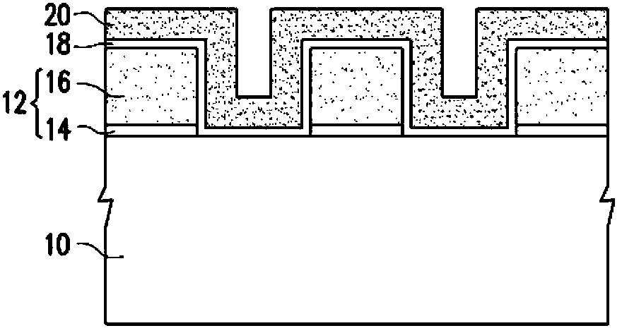
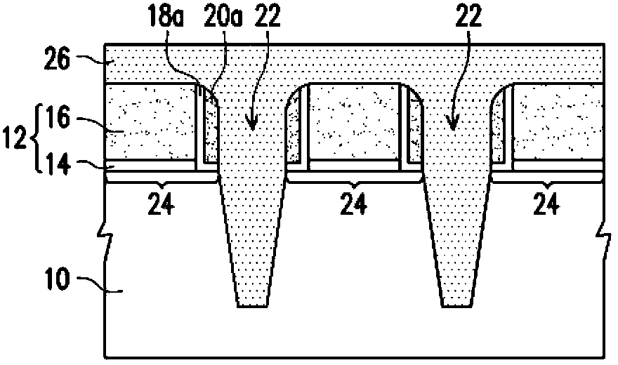
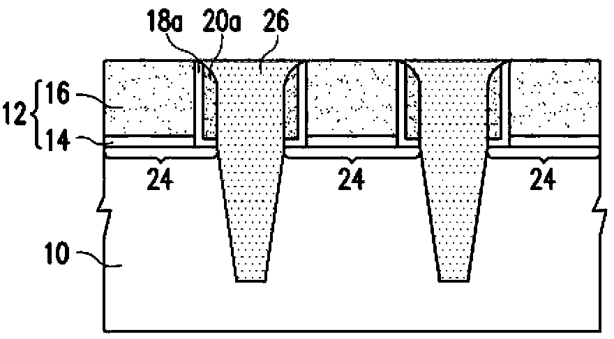
[0038] see Figure 1AAs shown, a patterned mask layer ...


PUM


Abstract

The invention relates to a nonvolatile memory cell and a manufacturing method of the nonvolatile memory cell. The nonvolatile memory cell comprises a substrate, electric charge storage structures and a tunneling dielectric layer. An isolation structure is arranged in the substrate, active areas are defined, and the electric charge storage structures are arranged on the active areas respectively. The width of the bottom of each electric charge structure is equal to the width of the corresponding active area in essence, the first included angle between the side wall of each electric charge storage structure and the upper surface of the substrate is different from the second included angle between the side wall of each isolation structure and the upper surface of the substrate. The tunneling dielectric layer is arranged between the electric charge storage structures and the substrate, the lower surface of the tunneling dielectric layer is flat, and the upper surface of the tunneling dielectric layer is parallel to the upper surface of the substrate in essence.

Description

technical field [0001] The invention relates to an integrated circuit and its manufacturing method, in particular to a non-volatile memory cell and its manufacturing method. Background technique [0002] Non-volatile memory allows multiple data programming, reading, and erasing operations, and the data stored in it can be preserved even after the memory's power supply is interrupted. Due to these advantages, non-volatile memory has become a widely used memory in personal computers and electronic equipment. [0003] Well-known electrically programmable and erasable nonvolatile memory technologies using charge storage structures, such as Electronically Erasable Programmable Read-Only Memory (EEPROM) and flash memory Body (flash memory), has been used in various modern applications. Flash memory is designed with an array of memory cells that can be programmed and read independently. A typical flash memory cell stores charge in a floating gate. Another non-volatile memory si...

Claims


Application Information

Patent Timeline
Patent Type & Authority Applications(China)
IPC IPC(8): H01L27/115H01L21/8247
Inventor 马处铭
Owner MACRONIX INT CO LTD
Why Eureka
Try Eureka