Method for fabricating mos device

a metaloxidesemiconductor and device technology, applied in the field of metaloxidesemiconductor (mos) device fabrication, can solve the problems of limited halo region and small process margin, and achieve the effect of improving the process margin of the implant process

Active Publication Date: 2013-07-18
UNITED MICROELECTRONICS CORP
View PDF19 Cites 17 Cited by
  • Summary
  • Abstract
  • Description
  • Claims
  • Application Information

AI Technical Summary

Benefits of technology

[0007]Accordingly, this invention provides a method for fabricating a MOS device, which allows the S / D extension regions and the halo regions to be formed in a uniform dopant concentration and a uniform depth and thus improve the process margin of the implant process of the S / D extension regions and the halo regions.
[0012]Since the implanted regions in the first (halo) implant process and the second (halo) implant process are different and the doses of the two processes can be controlled independently, the S / D extension regions (and the halo regions) each can be formed in a uniform dopant concentration and a uniform depth. Moreover, the implant angle of the first (halo) implant process is not much limited, so the process margin can be improved.

Problems solved by technology

However, in current FinFET process, the implant angle of the implant process for forming the source / drain (S / D) extension regions and the halo regions is much limited, so the process margin is very small.
Moreover, the S / D extension and the halo regions thus formed are uneven in dopant concentration and depth, and even cause leakage.

Method used


Image

  • Method for fabricating mos device
  • Method for fabricating mos device
  • Method for fabricating mos device

Examples


Embodiment Construction

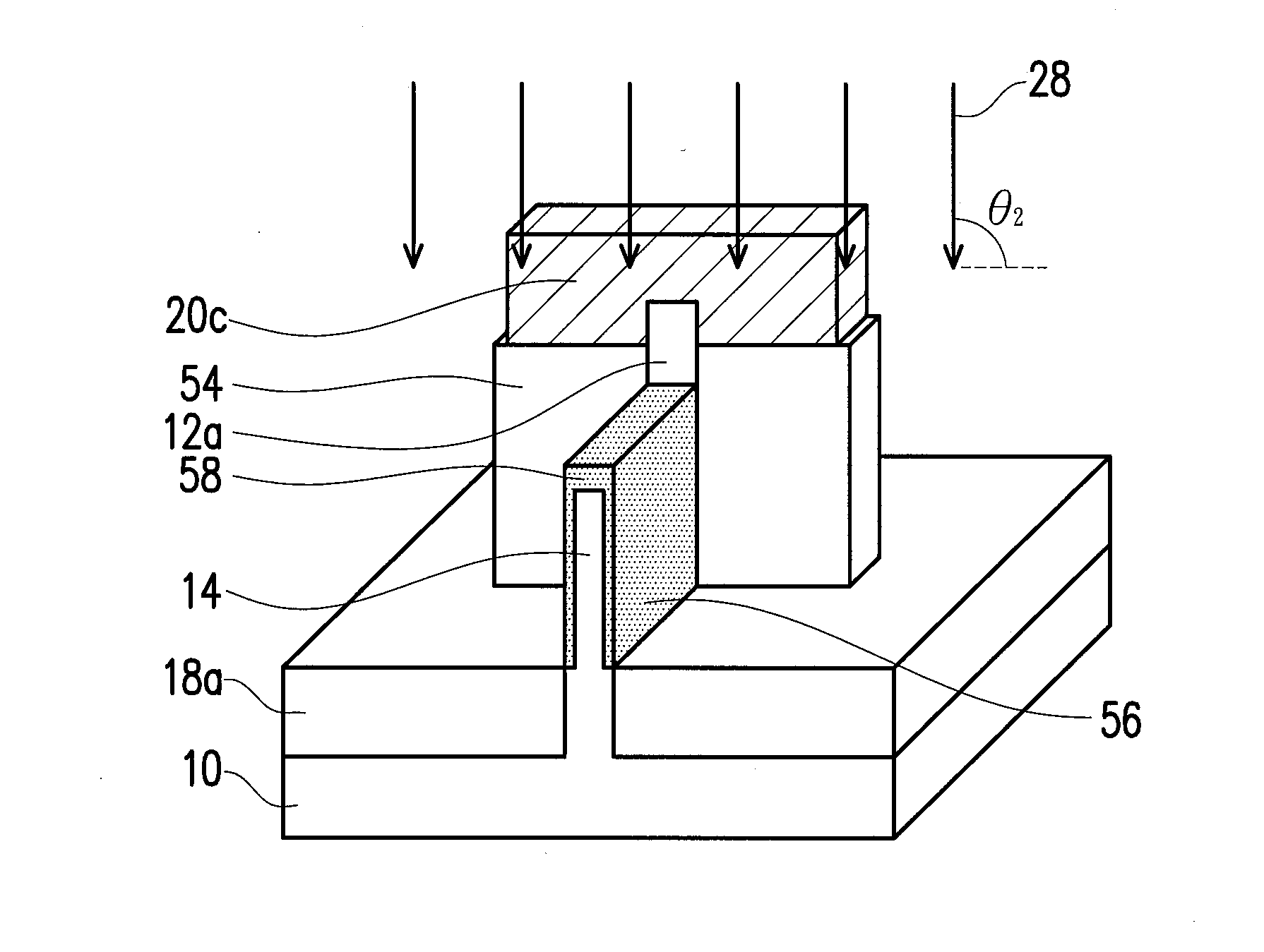
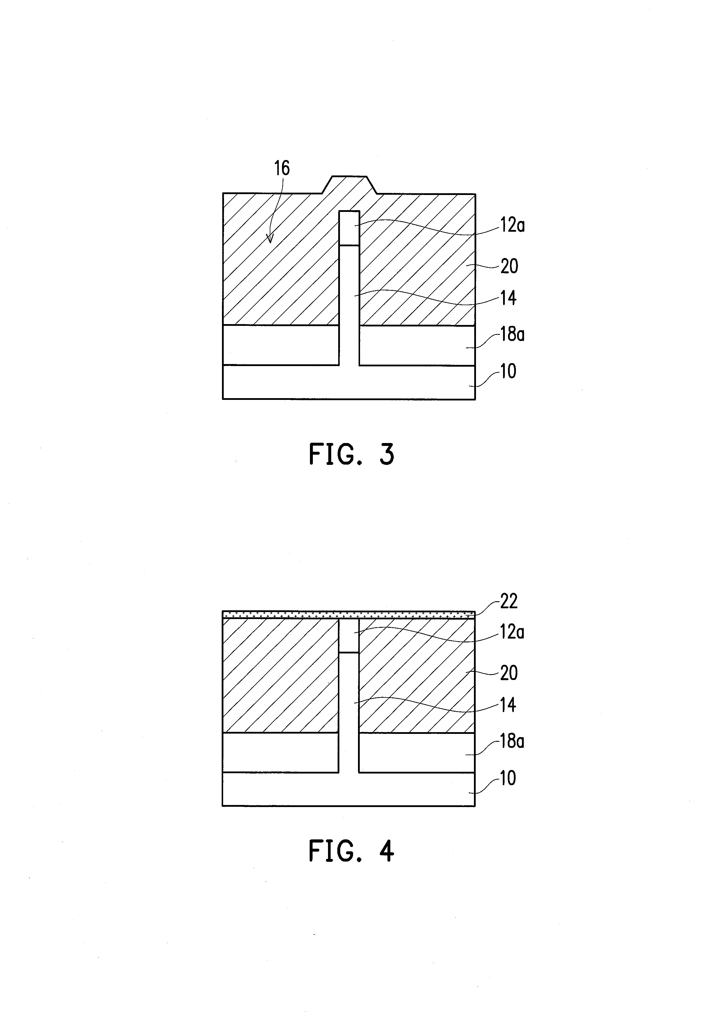
[0019]FIGS. 1-7 illustrate, in a side view along the first direction, a method for fabricating a MOS device according to an embodiment of this invention. FIGS. 8-11 illustrate, in a cross-sectional view along the second direction, further fabricating steps performed after the step shown in FIG. 7. FIGS. 5A-7A are perspective views of the structures shown in FIGS. 5-7.

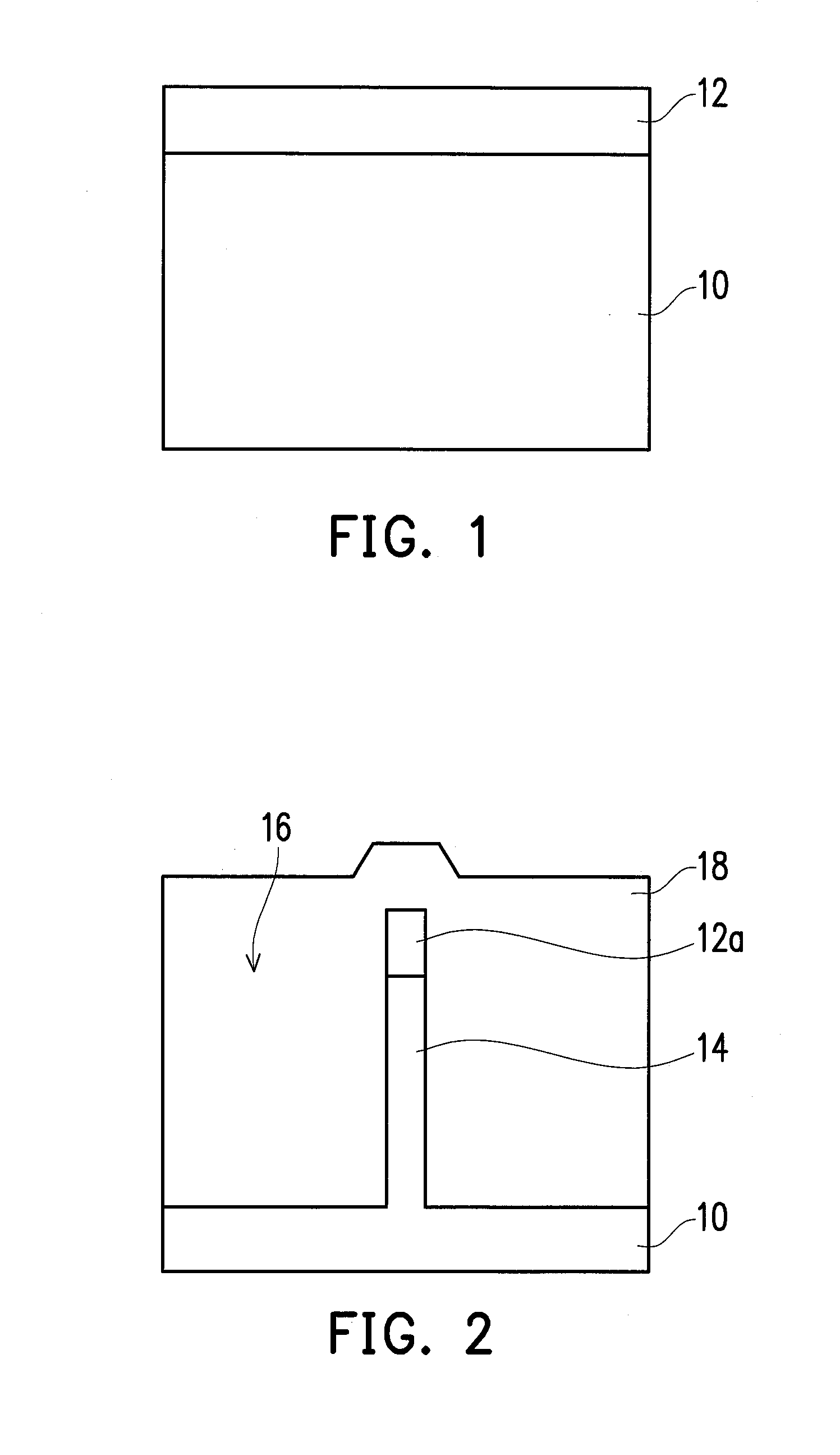
[0020]Referring to FIG. 1, a hard mask material layer 12 is formed over the substrate 10. The substrate 10 may include a semiconductor material, such as silicon. The hard mask material layer 12 may be a single material layer or include two or more material layers. In an embodiment, the hard mask material layer 12 includes a silicon dioxide (SiO2) layer and a silicon nitride (SiN) layer thereon. The SiO2 layer and the SiN layer can be formed by CVD. The SiO2 layer may have a thickness of 20-200 angstroms. The SiN layer may have a thickness of 500-3000 angstroms.

[0021]Referring to FIG. 2, lithography and etching processes...


PUM


Abstract

A method for fabricating a MOS device is described. A first hard mask layer is formed over a substrate. The first hard mask layer is patterned and a portion of the substrate removed to form a first patterned hard mask, and a fin structure surrounded by a trench and extending in a first direction. An insulating layer is formed at the trench bottom. A gate conductive layer is formed on the insulating layer, extending in a second direction. A first implant process is performed using the first patterned hard mask as a mask to form first S / D extension regions in the sidewalls of the fin structure. The first patterned hard mask is removed to expose the top of the fin structure, and then a second implant process is performed to form second S / D extension region therein.

Description

BACKGROUND OF THE INVENTION[0001]1. Field of Invention[0002]This invention relates to a semiconductor process, and more particularly relates to a method for fabricating a metal-oxide-semiconductor (MOS) device.[0003]2. Description of Related Art[0004]MOS is a basic structure widely applied to various semiconductor devices, such as memory devices, image sensors and display devices.[0005]The traditional MOS transistor is difficult to scale down due to the limitation of the fabricating process, so multi-gate transistors with better properties are developed. One example is the fin field-effect transistor (FinFET), which has a 3D gate structure to enhance the control on the channel and inhibit the leakage caused by the punch-through effect, and hence has a higher gate control ability than the conventional MOS transistor.[0006]However, in current FinFET process, the implant angle of the implant process for forming the source / drain (S / D) extension regions and the halo regions is much limit...

Claims


Application Information

Patent Timeline
Patent Type & Authority Applications(United States)
IPC IPC(8): H01L21/336
CPCH01L29/66803
Inventor WANG, CHIH-JUNGCHEN, TONG-YU
Owner UNITED MICROELECTRONICS CORP
Why Eureka
Try Eureka