Fingerprint image entry device of electrostatic capacitance sensing type

a technology of electrostatic capacitance and entry device, which is applied in the field of fingerprint image entry device of electrostatic capacitance sensing type, can solve the problems of hard to maintain reliability and safety of the device for an extended period of time, and hard to conduct accurate capacitance sensing

Inactive Publication Date: 2000-04-25
VISTA PEAK VENTURES LLC
View PDF9 Cites 59 Cited by
  • Summary
  • Abstract
  • Description
  • Claims
  • Application Information

AI Technical Summary

Benefits of technology

However, the above-mentioned prior art fingerprint image entry device has a problem that it is very hard to conduct accurate capacitance sensing. The reason is as follows:

Problems solved by technology

However, the above-mentioned prior art fingerprint image entry device has a problem that it is very hard to conduct accurate capacitance sensing.
Since the electrostatically charged condition of the finger may vary, it is practically hard to conduct accurate capacitance sensing.
In this case, it is hard to protect the grounding electrode from being damaged, resulting in a difficulty to maintain reliability and safety of the device for an extended period of time.

Method used


Image

  • Fingerprint image entry device of electrostatic capacitance sensing type
  • Fingerprint image entry device of electrostatic capacitance sensing type
  • Fingerprint image entry device of electrostatic capacitance sensing type

Examples


embodiment 1

[Embodiment 1]

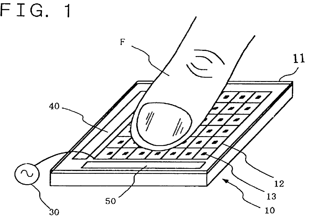
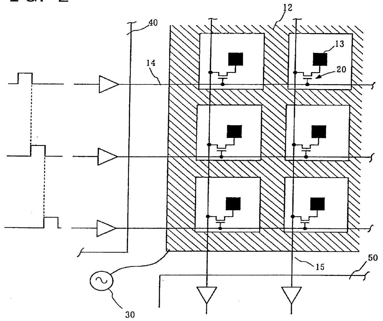
FIG. 1 is a perspective view showing a first embodiment of a fingerprint image entry device of the present invention. Referring now to FIG. 1, the fingerprint image entry device comprises a signal generating and detecting substrate 10 having a dielectric substrate 11 on which a signal generating electrode 12, a shift register circuit 40, and a signal sensing circuit 50 and the like are formed; and a high frequency signal generating source 30 which is connected to the signal generating electrode 12. FIG. 2 is an explanatory view schematically showing the configuration of the embodiment. FIG. 3 is an explanatory view explaining the configuration and operation of the embodiment.

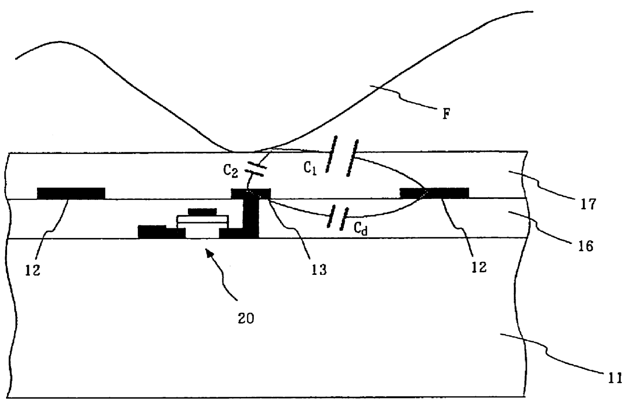
As shown in FIGS. 2 and 3, the signal generating and sensing substrate 10 comprises a plurality of thin film transistors which are two-dimensionally arrayed on the dielectric substrate 11, a first dielectric layer 16 formed on the substrate 11; signal sensing electrodes 13 formed on the dielectric ...

embodiment 2

[Embodiment 2]

FIG. 5 is an explanatory view showing the configuration of a second embodiment of the fingerprint image entry device of the present invention. In FIG. 5, the components which are like to those in FIG. 2 are represented by like reference numerals. Although the fingerprint image entry device comprises one signal generating electrode and a plurality of signal sensing electrodes in the foregoing first embodiment, the functions of these electrodes are exchanged with each other in the second embodiment of the present invention so that the fingerprint image entry device comprises one signal sensing electrode and a plurality of signal generating electrode.

Referring now to FIG. 5, the fingerprint image entry device of the second embodiment of the present invention comprises a plurality of thin film transistors 20 which are two-dimensionally arrayed, signal generating electrodes 22, a bank of leads 14 for connecting the gate electrodes of the thin film transistors to a first shi...

embodiment 3

[Embodiment 3]

FIG. 6 is an explanatory view showing the configuration of a third embodiment of the fingerprint image entry device of the present invention. In FIG. 6, the components which are like to those in FIG. 2 are represented by like reference numerals. Referring now to FIG. 6, the third embodiment of the present invention is substantially identical with the first embodiment except that the signal generating electrode 25 is divided into a plurality of elongated rectangular strips and that each signal generating electrode 25 is electrically connected to the signal generating source 30 in the same timing relationship as that the voltage of the lead 14 for the gate electrode in the same row is set to a high level by means of the shift register circuit 40.

Now, operation of the third embodiment of the present invention will be described.

When the output voltage of the shift register circuit 40 in the first row is set to a high level, a switching element 27 becomes conductive so that...


PUM


Abstract

Fingerprint image entry device having no ground electrode provided in a position with which a finger is in a direct contact, wherein accurate fingerprint image can be entered independently of the initial electrostatically charged condition of the finger. The device comprises an electrode which is in the form of mesh or comb for radiating a high frequency wave toward a finger, a plurality of signal sensing electrodes for forming electrostatic capacitance between the electrodes and the finger and a signal switching means for consecutively connecting each of these signal sensing electrodes to a signal sensing circuit.

Description

The present invention relates to an electrostatic capacitance coupling type fingerprint image entry device.The electrostatic capacitance sensing type fingerprint image input device is known from, for example, JP Patent Kokai Publication JP-A-8-305832. FIG. 8 is a perspective view showing the configuration of the electrostatic capacitance sensing type fingerprint image entry device which is disclosed in the cited JP Patent Kokai Publication JP-A-8-305832.Referring now to FIG. 8, this fingerprint entry device comprises a substrate 111 and a multiplicity of electrodes 112 and switching elements 113, which are two-dimensionally arrayed on the substrate 111. The electrodes 112 and switching elements 113 are connected to an electrostatic capacitive sensing circuit 116 and drive circuit 117 via Y leads 114 and X leads 115, respectively.Now, operation of the prior art fingerprint image entry device which is shown in FIG. 8 will be described. When a finger F is brought closer to the substrat...

Claims


Application Information

Patent Timeline
Patent Type & Authority Patents(United States)
IPC IPC(8): G06K9/00A61B5/117G01B7/28G06T1/00
CPCG06K9/0002G06V40/1306
Inventor FUJIEDA, ICHIRO
Owner VISTA PEAK VENTURES LLC
Why Eureka
Try Eureka