Design rule check method

a design rule and check method technology, applied in computer aided design, semiconductor/solid-state device testing/measurement, instruments, etc., can solve the problems of manual discrimination, difficult to obtain a correct inspection, and output of errors that do not meet this design standard

Inactive Publication Date: 2000-06-20
NEC ELECTRONICS CORP
View PDF3 Cites 59 Cited by
  • Summary
  • Abstract
  • Description
  • Claims
  • Application Information

AI Technical Summary

Problems solved by technology

In this case, when one design standard is present at one portion of mask pattern data, an error that does not satisfy this design standard is output directly.
When a plurality of design standards are present at one portion of mask pattern data, a plurality of errors not satisfying these design standards are output in contention, and it is difficult to obtain a correct inspection result. FIG. 1A shows such an example wherein a plurality of design standards are present at one portion of the mask pattern data.
The time required for making manual discrimination between a true error and a pseudo-error becomes necessary for the number of design rule check errors that recur, and a determination error can occur due to a human factor.
Occurrence of pseudo-errors cannot thus be prevented.
A time required for making manual determination between a true error and a pseudo-error becomes necessary for the number of design rule check errors that recur, and a determination error can occur due to a human factor, in the same manner as in the first conventional method.
The time required for making manual discrimination between a true error and a pseudo-error becomes necessary for the number of design rule check errors that recur, and a determination error can occur due to a human factor, in the same manner as in the conventional methods described above.

Method used


Image

  • Design rule check method
  • Design rule check method
  • Design rule check method

Examples


Embodiment Construction

A preferred embodiment of the present invention will be described with reference to the accompanying drawings.

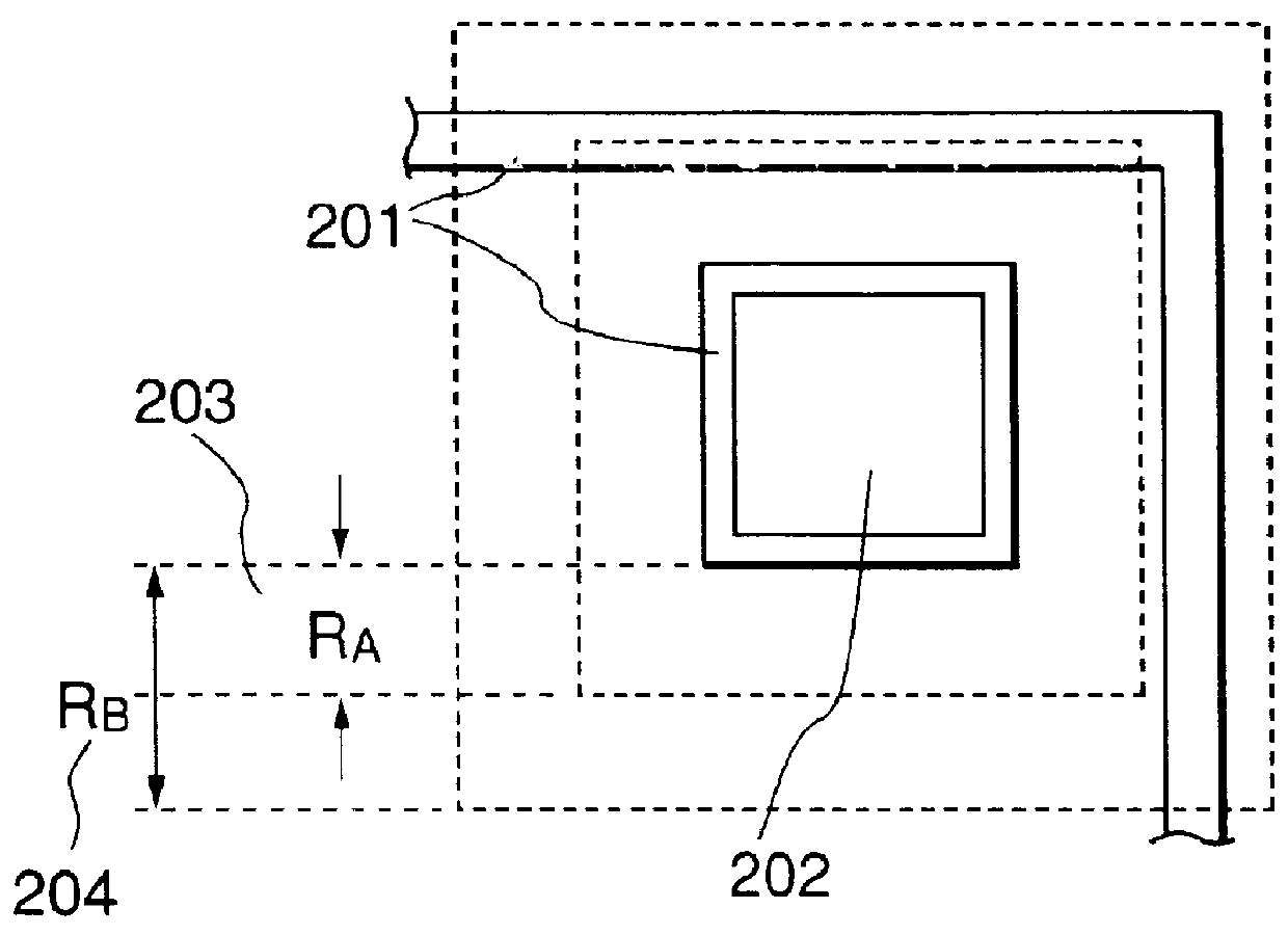
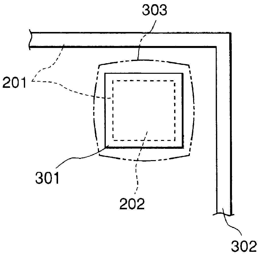
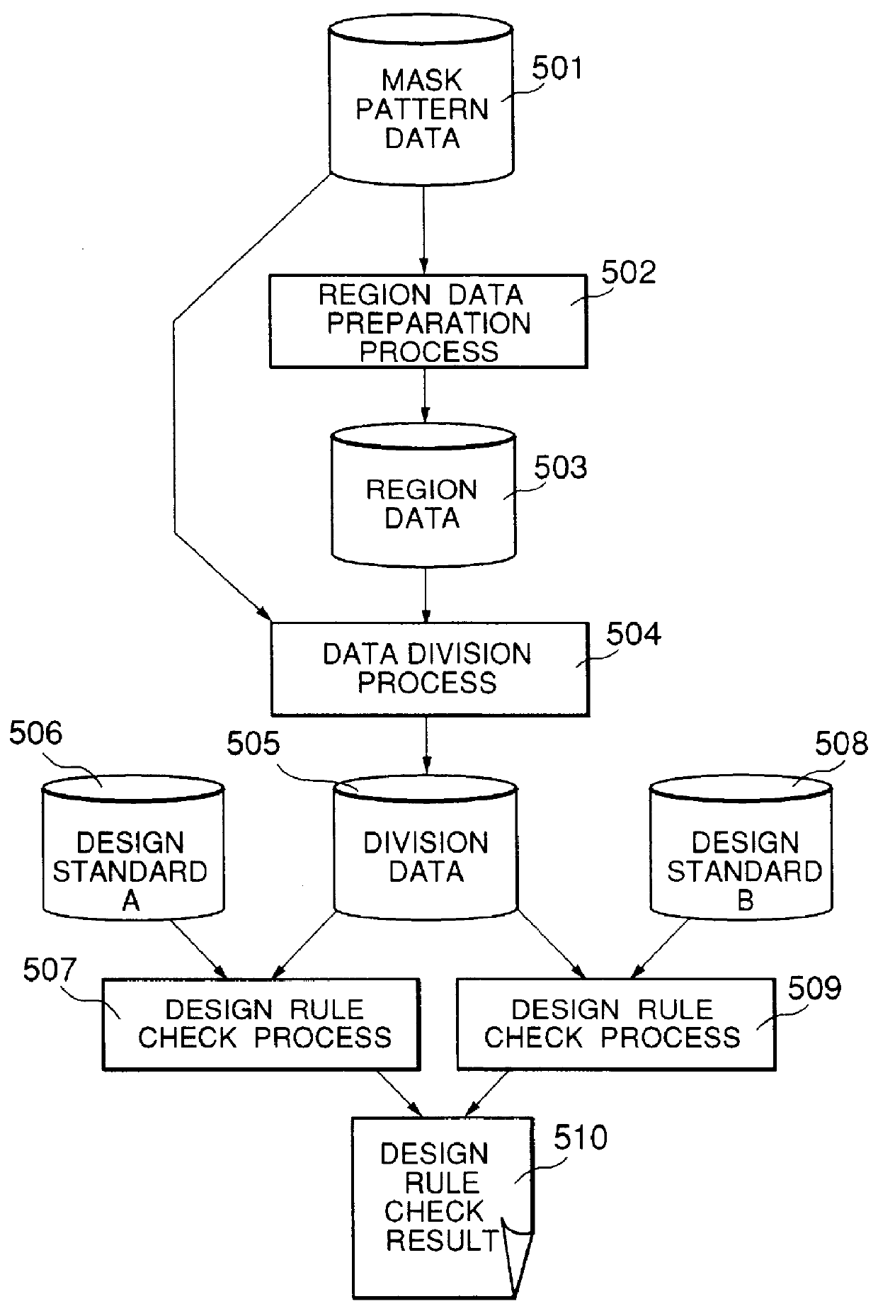
FIG. 12 is a block diagram showing the process according to an embodiment of the present invention by means of its steps. In this embodiment, the present invention is applied to a design rule check of mask pattern data that concerns a wiring line of the pad portion and a wiring line outside the pad portion, in the same manner as in the conventional technique described above. More specifically, mask pattern data 101 stores the mask pattern data shown in FIG. 4, in the same manner as in the conventional technique described above. Design standard A 102 stores a design rule consisting of a regulation value R.sub.A 203 as the spacing between the wiring line 301 of the pad portion and the wiring line 302 outside the pad portion which are described in the design standard example. Assume that design standard B 105 stores a design rule consisting of a regulation value R.sub.B 204 as ...


PUM


Abstract

A design rule check is to inspect whether mask pattern data of a semiconductor integrated circuit is correctly designed in accordance with a design standard or not. A design rule check method of the present invention is characterized in that design rule check errors occurring in the design rule check between a first error and a second error output in accordance with whether the design rule check errors overlap or not.

Description

1. Field of the InventionThe present invention relates to a design rule check with which whether mask pattern data is correctly designed in accordance with a pertinent design standard is inspected in the manufacture of a semiconductor integrated circuit and the like and, more particularly, to a design rule check method of determining and outputting a design rule check error and using it in correction of mask pattern data and the like.2. Description of the Prior ArtIn the manufacture of the semiconductor integrated circuit, whether or not the fabricated mask pattern complies with a predetermined design rule must be inspected prior to the actual manufacture of the semiconductor integrated circuit. In this case, when one design standard is present at one portion of mask pattern data, an error that does not satisfy this design standard is output directly. When a plurality of design standards are present at one portion of mask pattern data, a plurality of errors not satisfying these desi...

Claims


Application Information

Patent Timeline
Patent Type & Authority Patents(United States)
IPC IPC(8): G06F17/50H01L21/82H01L21/66
CPCG06F17/5081G06F30/398
Inventor SUZUKI, KYOU
Owner NEC ELECTRONICS CORP
Why Eureka
Try Eureka