Methods for cell boundary isolation in double patterning design

a double patterning and cell boundary technology, applied in the field of integrated circuit manufacturing processes, can solve the problems of double patterning technology not solving native conflict problems, features to short to each other, and the optical proximity effect posts an increasingly greater problem, so as to reduce the chip area usage of standard cells and reduce the design effort

Active Publication Date: 2012-08-28
TAIWAN SEMICON MFG CO LTD
View PDF10 Cites 18 Cited by
  • Summary
  • Abstract
  • Description
  • Claims
  • Application Information

AI Technical Summary

Benefits of technology

[0008]The advantageous features of the present invention include reduced design effort for achieving a native-conflict-free design. Further, chip area usage of standard cells is also reduced.

Problems solved by technology

With the increasing down-scaling of integrated circuits, the optical proximity effect posts an increasingly greater problem.
When two separate features are too close to each other, the optical proximity effect may cause the features to short to each other.
However, double patterning technology cannot solve native conflict problems.
When the cells, which may be free from native-conflict and free from rule violations, are put into the hierarchy of the circuits, the boundary features in neighboring cells may be too close to each other, and hence conflicts occur at this level.
In other words, there is no guarantee that the double-patterning rule compliance is still satisfied when the cells are integrated.

Method used


Image

  • Methods for cell boundary isolation in double patterning design
  • Methods for cell boundary isolation in double patterning design
  • Methods for cell boundary isolation in double patterning design

Examples


Embodiment Construction

[0016]The making and using of the embodiments are discussed in detail below. It should be appreciated, however, that the embodiments provide many applicable inventive concepts that can be embodied in a wide variety of specific contexts. The specific embodiments discussed are merely illustrative of specific ways to make and use the invention, and do not limit the scope of the invention.

[0017]A novel double patterning design method and the respective double patterning mask sets are provided. The variations of the embodiment are then discussed. Throughout the various views and illustrative embodiments of the present invention, like reference numbers are used to designate like elements.

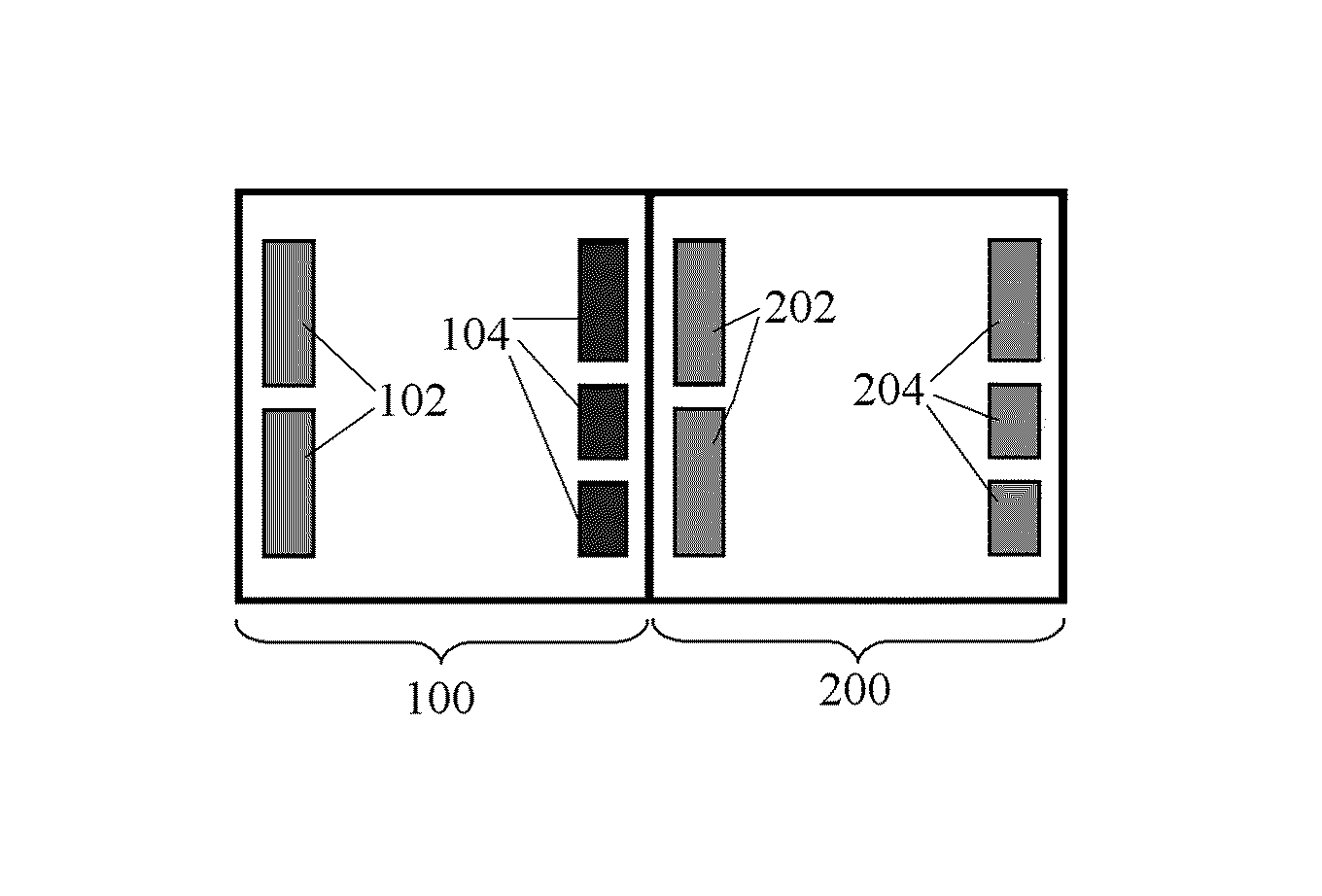
[0018]FIG. 4 illustrates an embodiment of the present invention, which includes cells 100 and 200 abutting each other. Cells 100 and 200 may be standard cells that may be saved in a cell library and copied into the layout of integrated circuits. The standard cells may include, but are not limited to, inve...


PUM


Abstract

A method of designing a double patterning mask set for a layout of a chip includes designing standard cells. In each of the standard cells, all left-boundary patterns are assigned with one of a first indicator and a second indicator, and all right-boundary patterns are assigned with an additional one of the first indicator and the second indicator. The method further includes placing the standard cells in a row of the layout of the chip. Starting from one of the standard cells in the row, indicator changes to the standard cells are propagated throughout the row. All patterns in the standard cells having the first indicator are transferred to a first mask of the double patterning mask set. All patterns in the standard cells having the second indicator are transferred to a second mask of the double patterning mask set.

Description

[0001]This application claims the benefit of U.S. Provisional Application No. 61 / 149,627 filed on Feb. 3, 2009, entitled “Methods for Cell Boundary Isolation in Double Patterning Design,” which application is hereby incorporated herein by reference.TECHNICAL FIELD[0002]This invention relates generally to integrated circuit manufacturing processes, and more particularly to using double patterning technology to reduce the lithography limits of integrated circuits.BACKGROUND[0003]Double patterning is a technology developed for lithography to enhance the feature density. Typically, for forming features of integrated circuits on wafers, lithography technology is used, which involves applying a photo resist, and defining patterns on the photo resist. The patterns in the patterned photo resist are first defined in a lithography mask, and are defined either by the transparent portions or by the opaque portions in the lithography mask. The patterns in the patterned photo resist are then tran...

Claims


Application Information

Patent Timeline
Patent Type & Authority Patents(United States)
IPC IPC(8): G06F17/50
CPCG03F1/144G03F1/00G03F1/70
Inventor LU, LEE-CHUNGCHENG, YI-KANHOU, YUAN-TEHOU, YUNG-CHINTIEN, LI-CHUN
Owner TAIWAN SEMICON MFG CO LTD
Why Eureka
Try Eureka