Salphasic timing calibration system for an integrated circuit tester

a timing calibration and integrated circuit technology, applied in the field of integrated circuit testers, can solve the problems of time-consuming manual process, difficult, tedious and laborious

Inactive Publication Date: 2000-08-15
CREDENCE SYSTEMS
View PDF13 Cites 89 Cited by
  • Summary
  • Abstract
  • Description
  • Claims
  • Application Information

AI Technical Summary

Problems solved by technology

Unfortunately measuring those signal path delays, typically through the use of oscilloscopes or other t

Method used


Image

  • Salphasic timing calibration system for an integrated circuit tester
  • Salphasic timing calibration system for an integrated circuit tester
  • Salphasic timing calibration system for an integrated circuit tester

Examples


Embodiment Construction

)

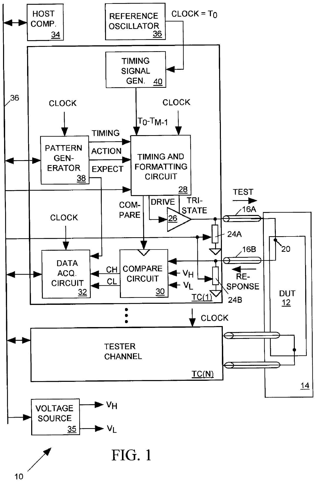
Integrated Circuit Tester Architecture

FIG. 1 illustrates an integrated circuit tester 10 for performing a digital logic test on an integrated circuit device under test (DUT) 12 mounted on a printed circuit load board 14. Tester 10 includes a set of N tester channels TC(1)-TC(N). Each channel TC(1)-TC(N) is connected to a separate terminal of DUT 12 through a pair of transmission lines 16A and 16B, each including a remote end for contacting a DUT terminal 20 so that each transmission line may convey signals between the DUT terminal and the tester channel. Transmission lines 16A and 16B have similar characteristic impedances normally matched by a programmable terminating impedance 24A or 24B to prevent signal reflections. Host computer 34 may adjust the impedance of impedance system 24 of each channel TC(1)-TC(N) by sending control data to impedances 24A and 24B via bus 36.

Each DUT terminal 20 may be either an input terminal, and output terminal or both an input and an output termina...


PUM


Abstract

An integrated circuit tester produces an output TEST signal following a pulse of a reference CLOCK signal with a delay that is a sum of an inherent drive delay and an adjustable drive delay. The tester also samples an input RESPONSE signal following a pulse of the reference CLOCK signal with a delay that is a sum of an inherent compare delay and an adjustable compare delay. The inherent drive and compare signal path delays within an integrated circuit tester are measured by first connecting a salphasic plane to transmission lines that normally convey signals between the tester and terminals of an integrated circuit device under test. A standing wave signal appearing on that salphasic plane is phase locked to the CLOCK signal so that a zero crossing of the standing wave occurs at a fixed interval after each pulse of the CLOCK signal. Each transmission line concurrently conveys the standing wave to the tester to provide timing references for measuring the inherent drive and compare signal path delays within the tester. Transmission line signal paths are also measured. Delays are added to the drive and compare signal paths to compensate for the measured inherent drive, compare and transmission line delays.

Description

1. Field of the InventionThe present invention relates in general to integrated circuit testers and in particular to a tester employing a salphasic plane when self-calibrating its signal timing.2. Description of Related ArtA typical integrated circuit tester tests a digital logic integrated circuit device under test (DUT) by applying test signals of various logic states to DUT input terminals and by monitoring states of signals produced at DUT output terminals in response to the test signals to determine whether the DUT is behaving as expected. Such a tester typically includes a set of tester channels, each connected to a separate terminal of the DUT, and each carrying out all test activities with respect to that DUT terminal. A test is typically organized into a succession of test cycles. Each channel receives input ACTION and TIMING data for each test cycle telling the channel what actions to take during the test cycle and indicating the times during the test cycle at which it is ...

Claims


Application Information

Patent Timeline
IPC IPC(8): G01R31/28G01R31/319
CPCG01R31/3191
Inventor MILLER, CHARLES A.
Owner CREDENCE SYSTEMS
Why Eureka
Try Eureka