Semiconductor substrate subassembly with alignment and stress relief features

Inactive Publication Date: 2000-10-03
DELPHI TECH IP LTD
View PDF25 Cites 61 Cited by
  • Summary
  • Abstract
  • Description
  • Claims
  • Application Information

AI Technical Summary

Benefits of technology

As with the semiconductor substrate subassembly of U.S. Pat. No. 5,492,842 and U.S. Pat. No. 5,539,254, the improved subassembly of this invention permits one to obtain a high degree of electrical symmetry among switching transistors grouped in a module, and in their electrical connections to module terminal members. These connections have low parasitic impedance loses because they are quite short.

Problems solved by technology

On the other hand, the high current density capability and low "on" resistance of the IGBT also present challenges.
The possibility of device failure is aggravated when the IGBT is handling high power.
As might be expected, significant impedance, material and mechanical proble

Method used


Image

  • Semiconductor substrate subassembly with alignment and stress relief features
  • Semiconductor substrate subassembly with alignment and stress relief features
  • Semiconductor substrate subassembly with alignment and stress relief features

Examples


Example

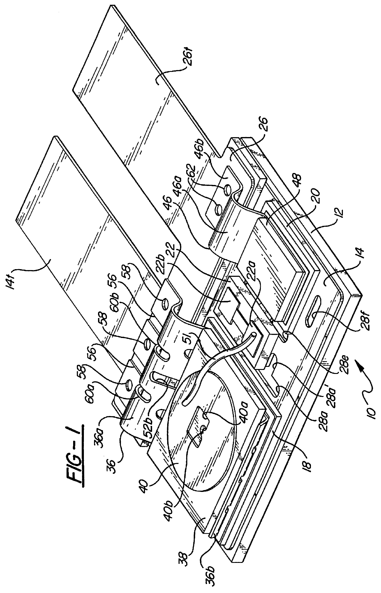
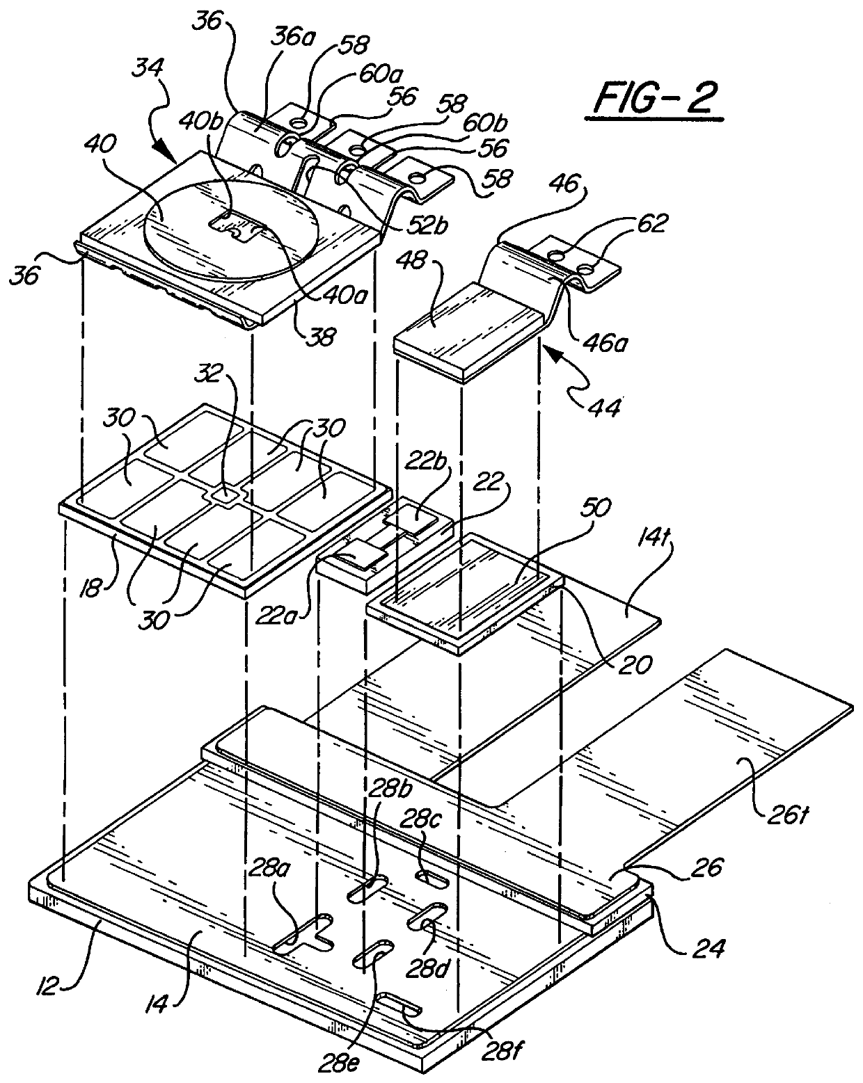
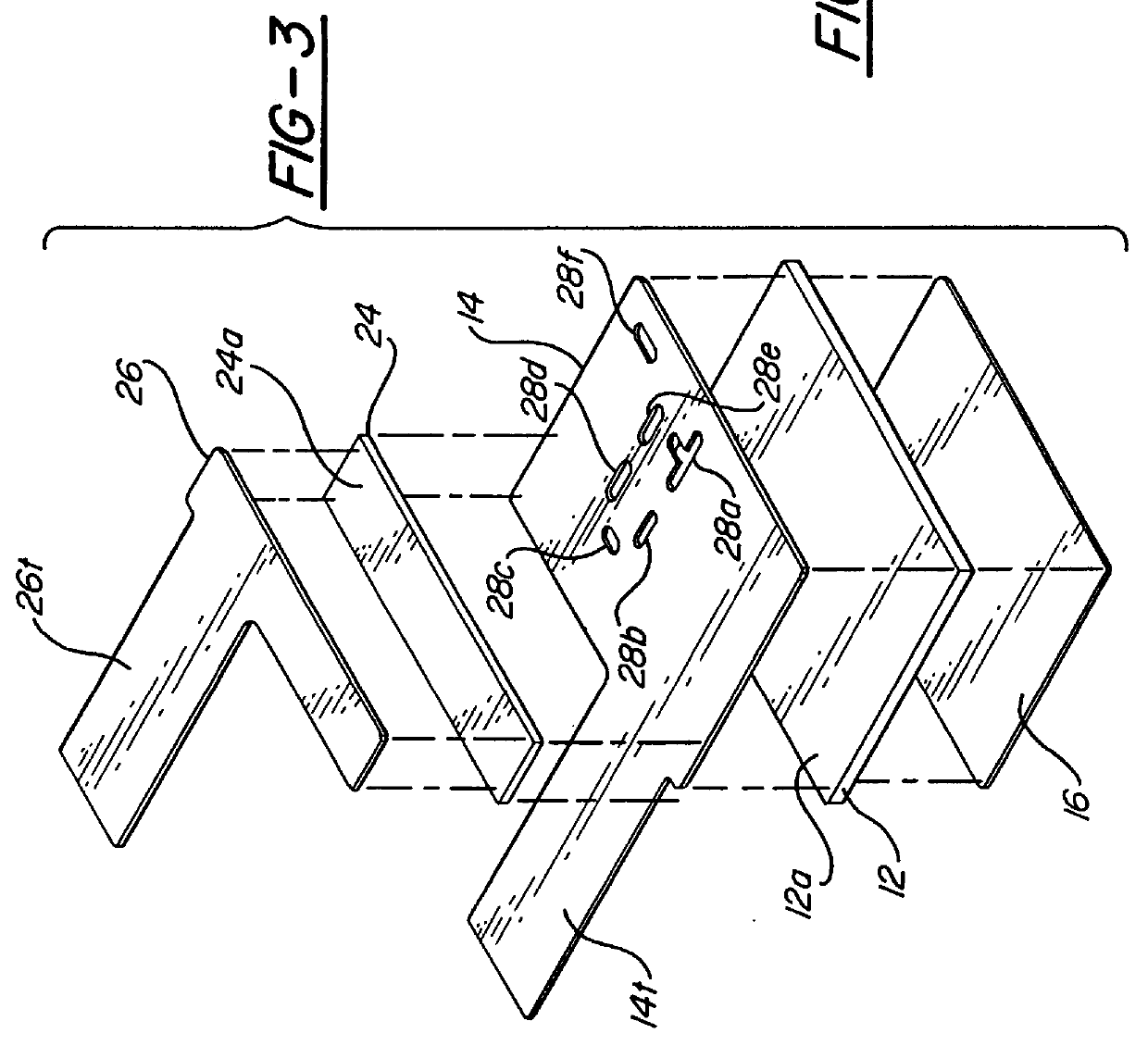
As with the substrate subassemblies of U.S. Pat. No. 5,492,842 and U.S. Pat. No. 5,539,254, the substrate subassemblies of this invention can be used in a concentric single and dual switch modules, as well as in linear single and dual switch modules, which are described in those and the other related patents identified above.

This description describes details of the improved semiconductor contact system, which has a particularly special utility in a high substrate subassembly. For completeness, this description also contains a specific example of a module in which the improved substrate subassembly can be used. The specific example is a linear dual module with coplanar inner terminal contacts, along the lines of the module described and claimed in U.S. Pat. No. 5,523,620 Eytcheson et al. However, it is to be understood that the subject substrate subassembly can be used in a variety of module types, including concentric single and dual switch modules, as are as described in U.S. Pat....


PUM


Abstract

A composite conductor for contacting a semiconductor device chip. A durable substrate subassembly for a high power transistor switching modules. The substrate subassembly is durable because wire bonds to the semiconductor device electrodes are replaced with a soldered metal/ceramic composite conductor. The part of the composite conductor contacting the semiconductor device has a coefficient of thermal expansion close to that of the semiconductor device. The substrate in the substrate subassembly has automatic alignment features. The composite conductor also has automatic alignment features, along with stress relief features. Automatic alignment permits concurrent soldering of the chip to the substrate, and the composite conductor to the chip and to a terminal contact.

Description

RELATED PATENTSThis patent application describes and claims a modification to the inventions described and claimed in U.S. Pat. Nos. 5,539,254 Eytcheson et al., issued Jul. 23, 1996, 5,523,620 Eytcheson et al., and 5,492,842 Eytcheson et al. issued Feb. 20, 1996. The foregoing U.S. patents are hereby incorporated herein by reference.This invention is also related to the following U.S. patents, which are also incorporated herein by reference: U.S. Pat. No. 5,563,447 Lake et al., issued Oct. 8, 1996; U.S. Pat. No. 5,519,253 Lake et al., issued May 21, 1996; U.S. Pat. No. 5,444,295 Lake et al., issued Aug. 22, 1995; U.S. Pat. No. 5,517,059 Eytcheson et al., issued May 14, 1996; and U.S. Pat. No. 5,512,790 Lachenmaier et al.This invention relates to packaging of a high voltage / high current / high frequency semiconductor switching device. More specifically, this invention relates to a distinctive subassembly containing such a switching device, and to a power module containing a plurality o...

Claims


Application Information

Patent Timeline
IPC IPC(8): H01L23/495H01L23/48
CPCH01L23/49562H01L24/36H01L25/18H01L24/40H01L2924/1305H01L2924/1306H01L2224/48472H01L2924/01004H01L2924/01013H01L2924/01029H01L2924/01079H01L2924/01082H01L2924/13055H01L2924/13091H01L2924/19043H01L2924/30105H01L2924/30107H01L2924/3011H01L24/48H01L2924/01033H01L2924/01047H01L2924/00H01L2924/15787H01L2224/40225H01L2224/05647H01L24/45H01L2224/45099H01L2224/45124H01L2224/85399H01L2924/00014H01L2224/40091H01L2224/37011H01L2224/37147H01L2224/83801H01L24/37H01L24/41H01L2224/0603H01L2224/84801H01L24/84H01L2224/45015H01L2924/207H01L2224/73221
Inventor EYTCHESON, CHARLES TYLER
Owner DELPHI TECH IP LTD
Why Eureka
Try Eureka