Electrical contact for a printed circuit board

a printed circuit board and contact technology, applied in the field of electric contact, can solve the problems of affecting the overall reliability of the board, the contact between the surface mount pad and the contact is at substantial risk of failure, and the surface mount pad contact is less structural integrity

Inactive Publication Date: 2001-01-30
EMC IP HLDG CO LLC
View PDF24 Cites 76 Cited by
  • Summary
  • Abstract
  • Description
  • Claims
  • Application Information

AI Technical Summary

Problems solved by technology

In addition to increasing the number of process steps, this process can impact the overall reliability of the board since the surface mount components and their solder joints are subjected to the thermal shock of the wave soldering process.
Surface mount pin contacts, however, tend to have less structural integrity than a through-hole contact.
Additionally, the solder joint between the surface mount pad and the contact is at substantial risk to fail, since the contact typically includes no support structure that would distribute forces applied to the contact away from the solder joint.
Surface mount electrical contacts used as test pins are particularly prone to structural and solder joint failures since they are typically subjected to relatively large forces when probed, grasped and interconnected during testing on a board.
The lack of support structure also makes it difficult to maintain a surface mount contact precisely positioned on a circuit board during the assembly process.

Method used


Image

  • Electrical contact for a printed circuit board
  • Electrical contact for a printed circuit board
  • Electrical contact for a printed circuit board

Examples


Embodiment Construction

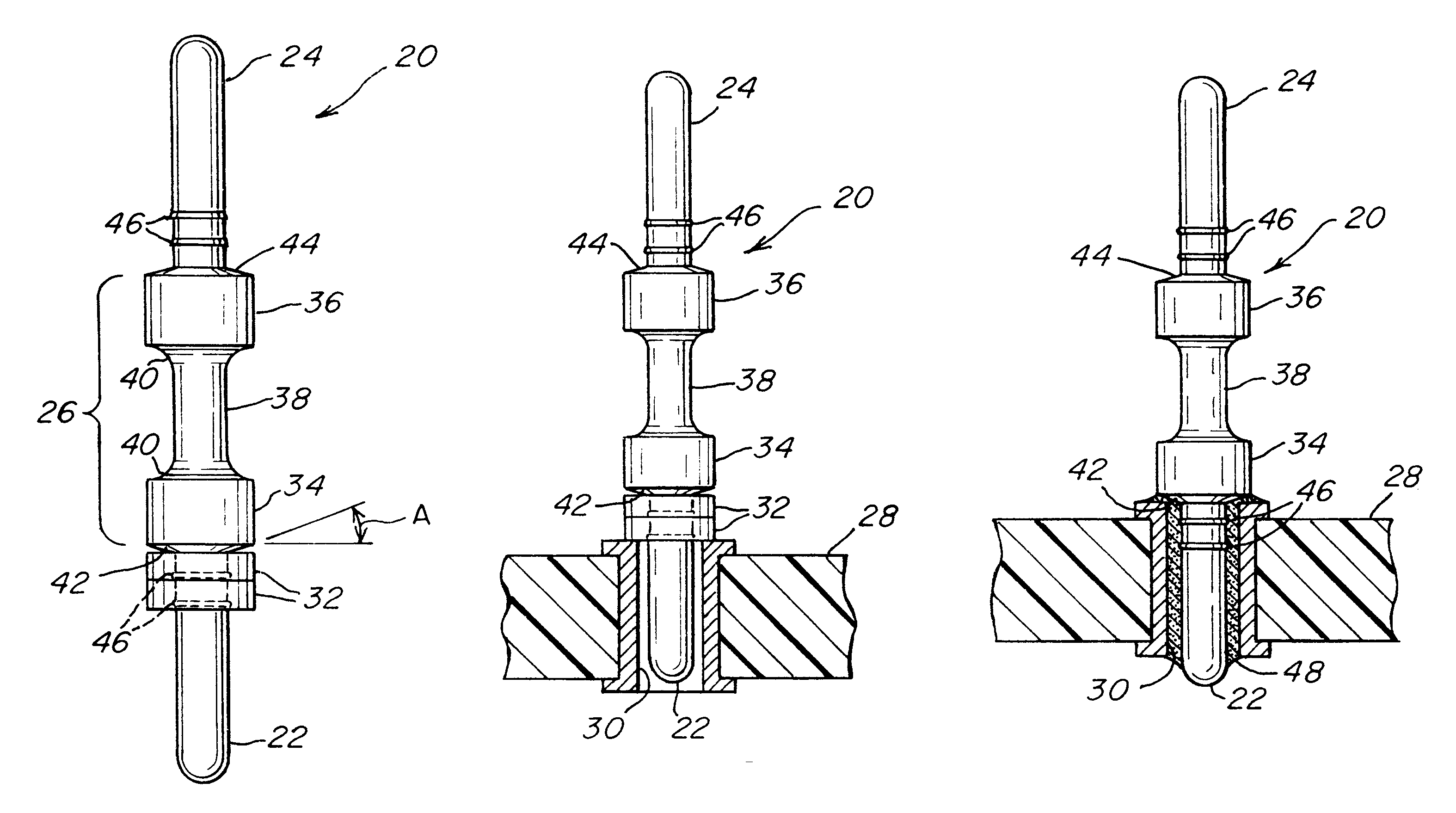
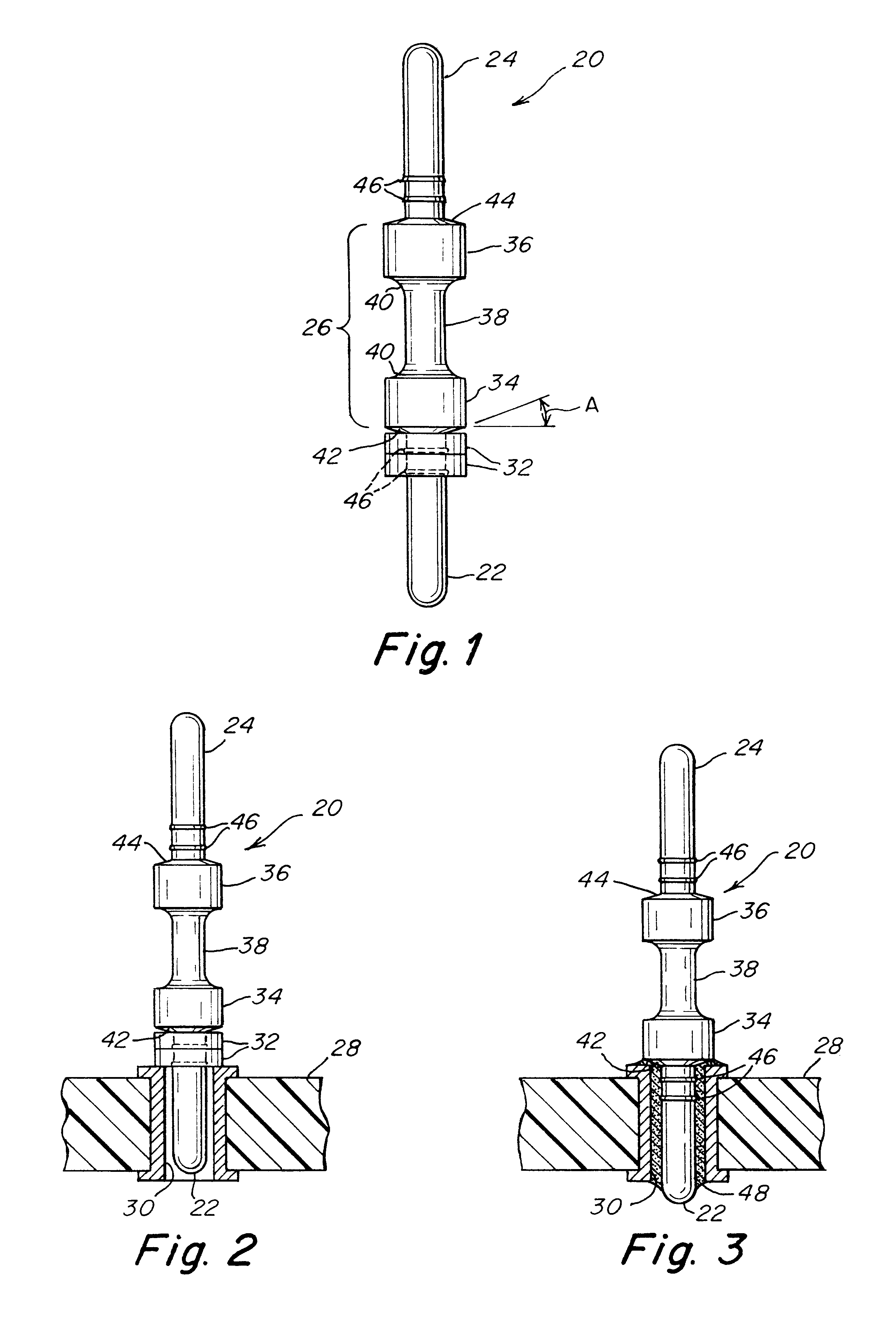
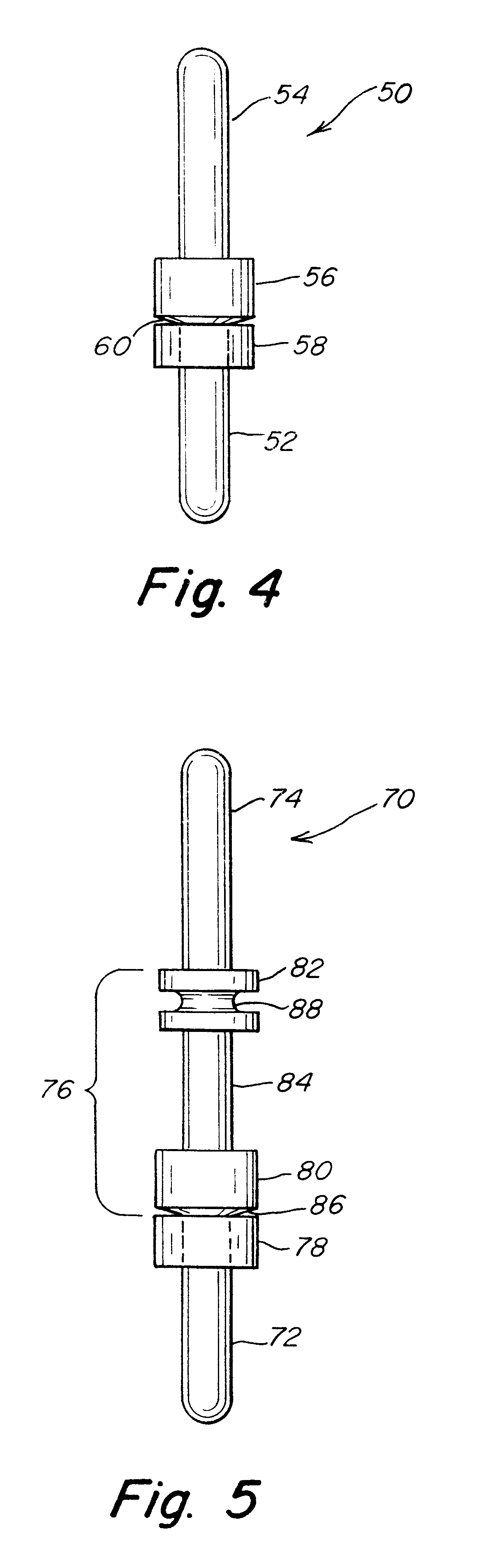
In accordance with one illustrative embodiment of the invention, an electrical contact is provided for being mounted on a printed circuit board to establish an electrical connection to the circuit board. The electrical contact may be inserted into a plated-through hole in the circuit board and soldered using a surface mount intrusive reflow process. The contact may be manually mounted or automatically mounted onto the board using an automated assembly process. To enhance automated assembly processes, a plurality of the electrical contacts may be provided in a component magazine or on a reel tape. It should be appreciated that the illustrative embodiments discussed below are provided merely for illustrative purposes, and that numerous other implementations are possible.

In one illustrative embodiment of the invention shown in FIGS. 1-3, the electrical contact 20 includes first and second elongated, conductive pins 22, 24 attached to first and second ends of a base 26 that is configure...


PUM


Abstract

An electrical contact that is mounted on a printed circuit board to provide an electrical connection to the printed circuit board. The contact has the structural integrity of a through-hole component with the capability of being soldered to the circuit board using a surface mount reflow process. The contact includes a pair of elongated, conductive pins with a base disposed therebetween, and a solder preform supported on one of the conductive pins adjacent the base. The pin supporting the solder preform is insertable into a plated-through hole on the circuit board so that the solder preform can be reflowed into the hole along the pin to form a solder joint between the contact and the hole. The contact may include a retainer to secure the solder preform to the pin and the end of the base adjacent the pin may be beveled to facilitate gas ventilation from the hole during the soldering process. The base may be configured so that it can be grasped with a test instrument or support a wire connection to the contact. The contact may be symmetrical so that the solder preform can be supported on either conductive pin.

Description

1. Field of the InventionThe present invention relates to an electrical contact, and more particularly to an electrical pin contact for mounting on a printed circuit board.2. Description of Related ArtElectrical pin contacts are typically mounted to a printed circuit board for establishing electrical interconnections to the circuitry of the board. For example, one or more contacts can be mounted to a circuit board to provide test pin connections that can be probed for testing or troubleshooting the board. Pin contacts can also provide an interface for an electrical connector or other socket-type device to interconnect a board to other electronic components.Electronic components, including pin contacts, are generally configured for mounting on a printed circuit board as either a surface mount component or a through-hole component. A surface mount component includes leads that are soldered directly to surface mount pads provided on the outer surfaces of the circuit board. Conventional...

Claims


Application Information

Patent Timeline
Patent Type & Authority Patents(United States)
IPC IPC(8): H01R43/02H05K3/34H01R12/58
CPCH01R9/091H01R43/0256H05K3/3447H05K2201/10303H05K2201/10871H05K2203/0415H01R12/58
Inventor DOWNES, STUART D.MERRILL, LEONARD A.
Owner EMC IP HLDG CO LLC
Why Eureka
Try Eureka