

Semiconductor device and method of fabricating the same
- Summary
- Abstract
- Description
- Claims
- Application Information
AI Technical Summary
Benefits of technology
Problems solved by technology
Method used
Image

Examples
first embodiment
[FIRST EMBODIMENT]
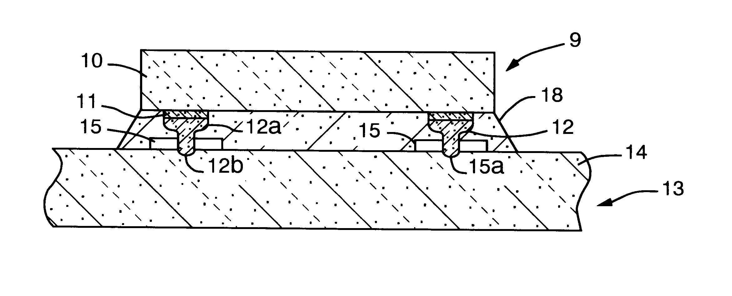
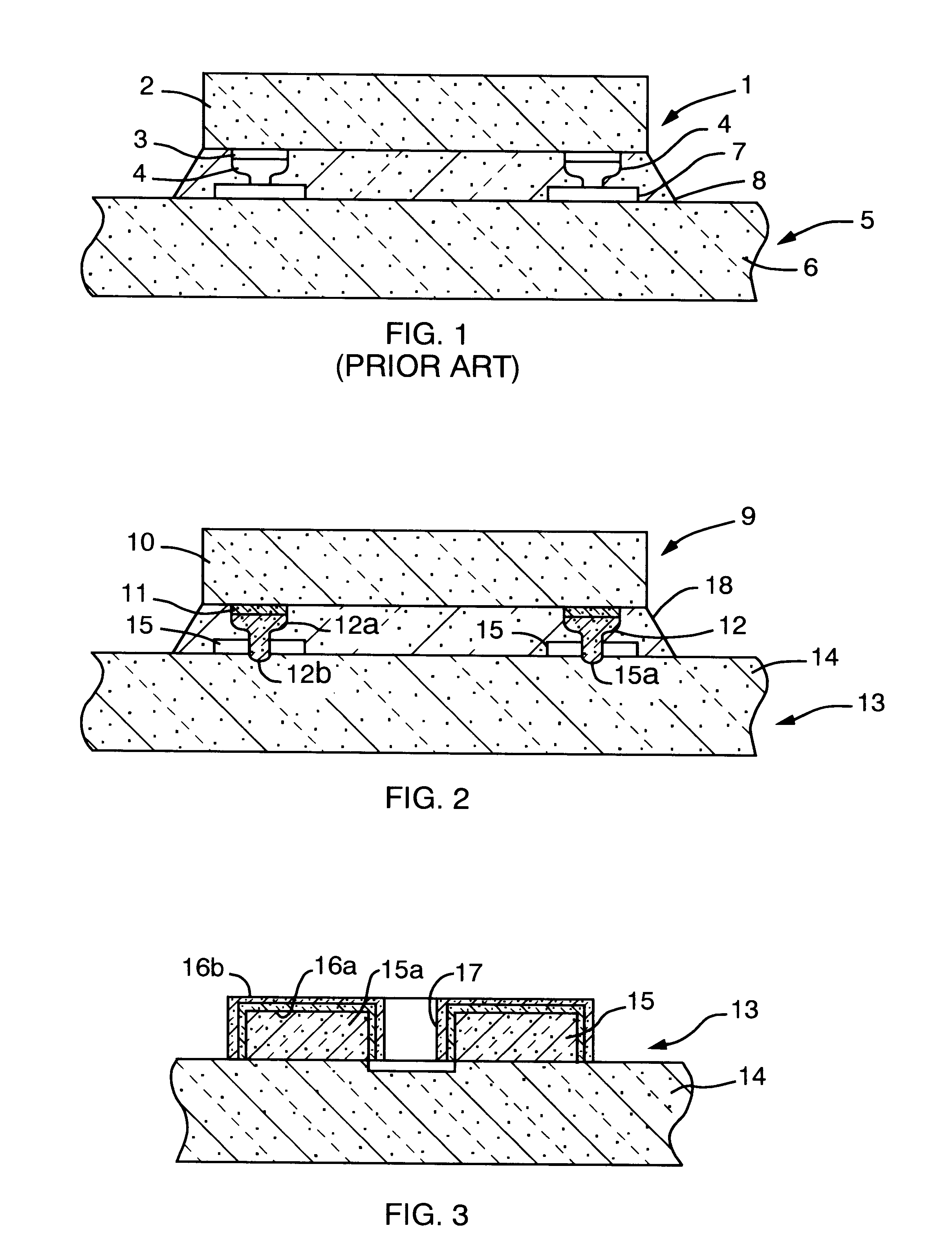
FIGS. 2 to 4 illustrate a semiconductor device in accordance with the first embodiment. With reference to FIG. 2, the illustrated semiconductor device is comprised of a semiconductor pellet 9, a wiring board 13 to be coupled to the semiconductor pellet 9, and a resin layer 18 sandwiched between the semiconductor pellet 9 and the wiring board 13 for enhancing engagement therebetween.
The semiconductor pellet 9 is comprised of a semiconductor substrate including a plurality of semiconductor elements (not illustrated) which are interconnected to one another to thereby constitute an electronic circuit, an insulating film (not illustrated) formed on a principal surface of the semiconductor substrate 10, underlying electrodes 11 formed in regions where the insulating film is partially removed, and making electrical connection with the semiconductor elements, and bump electrodes 12 formed on the underlying electrodes 11. The underlying electrodes 11 are made of aluminum.
In...
second embodiment
A period of time for the resin 18 to cure is dependent directly on a temperature at which the resin 18 is heated. Hence, there may be used a resin which cures in a shorter period of time. As an alternative, there may be used a resin which is cured by ultra-violet ray, to thereby save a time for curing a resin. It is also possible to heat the resin 18 at a temperature higher than 200.degree. C. in a shorter period of time. [Second Embodiment]
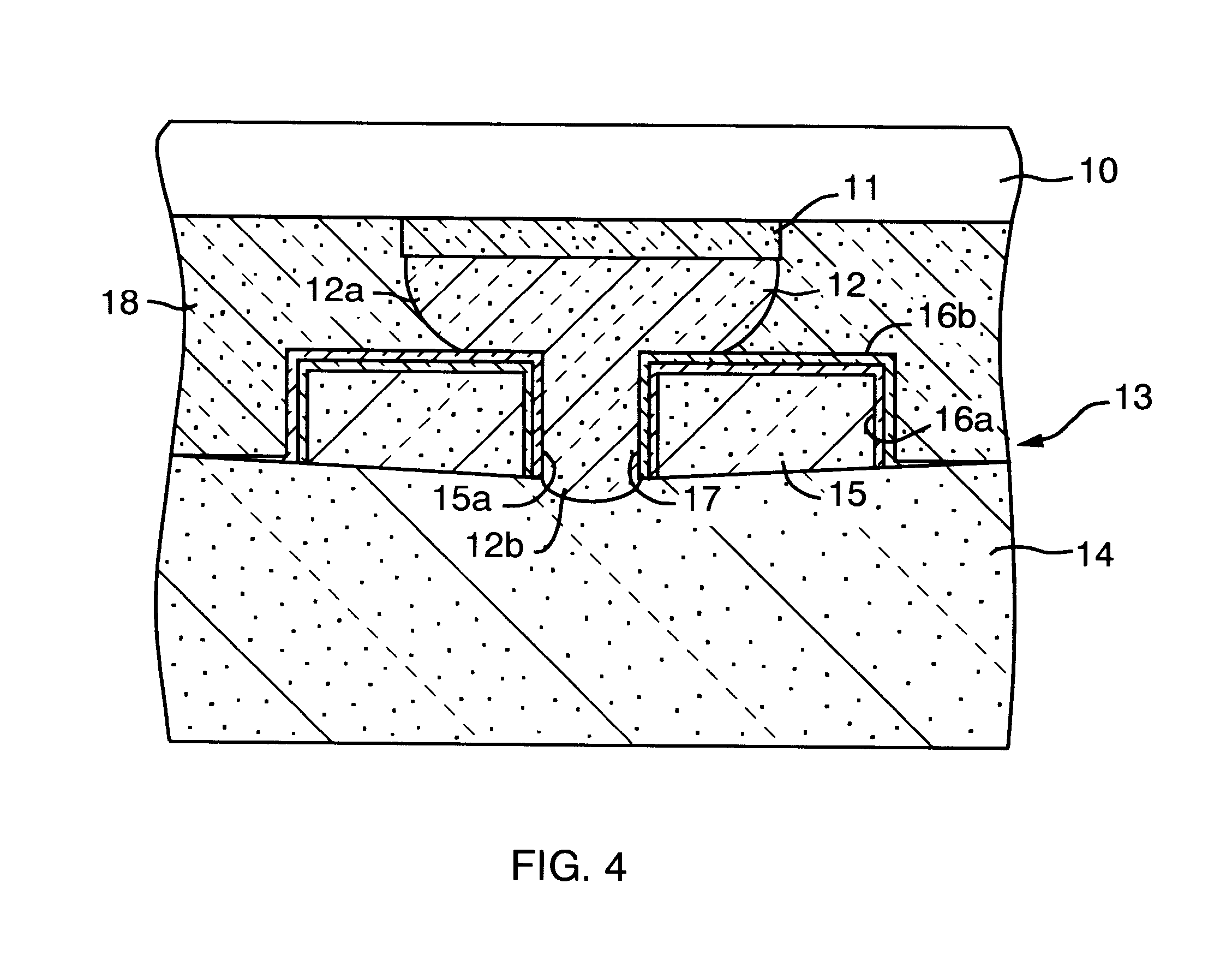
FIGS. 5 to 7 illustrate a semiconductor device in accordance with the second embodiment. With reference to FIG. 5, the illustrated semiconductor device is comprised of a semiconductor pellet 9, a wiring board 13 to be coupled to the semiconductor pellet 9, and a resin layer 18 sandwiched between the semiconductor pellet 9 and the wiring board 13 for enhancing engagement therebetween.
The semiconductor device in accordance with the second embodiment is almost the same as the first embodiment illustrated in FIGS. 2 to 4, but is different from the fi...
PUM
 Abstract
Description
Claims
Application Information