Display device

a display device and active matrix technology, applied in the direction of luminescnet screens, identification means, instruments, etc., can solve the problems of large parasitic capacitance associated with each data line, large load on the data line "sig" and other problems, to achieve the effect of large parasitic capacitance on the parasitic capacitance of each data lin

Inactive Publication Date: 2001-02-27
INTELLECTUAL KEYSTONE TECH LLC
View PDF3 Cites 351 Cited by
  • Summary
  • Abstract
  • Description
  • Claims
  • Application Information

AI Technical Summary

Problems solved by technology

As a result, the data lines "sig" have a large parasitic capacitance which causes the data lines "sig" to have a large load.
As a result, the data line driving circuit 3 also has a problem of a large load caused by the large parasitic capacitance.
This can result in a large parasitic capacitanc...

Method used


Image

  • Display device
  • Display device
  • Display device

Examples


Embodiment Construction

The present invention is described in further detail below with reference to embodiments in conjunction with the accompanying drawings.

(General Construction of Active Matrix Substrate)

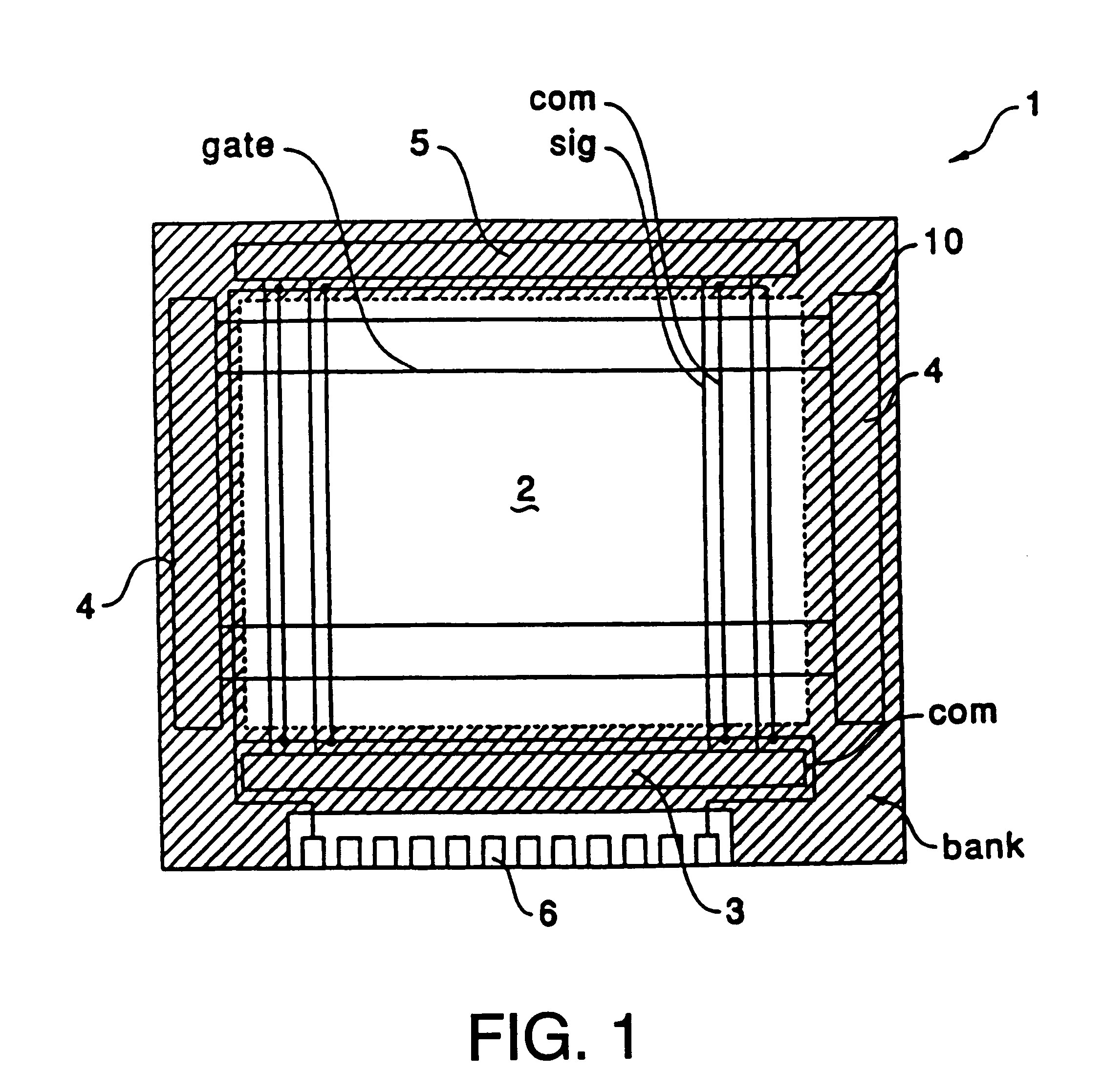
FIG. 1 is a block diagram schematically illustrating the general layout of a display device.

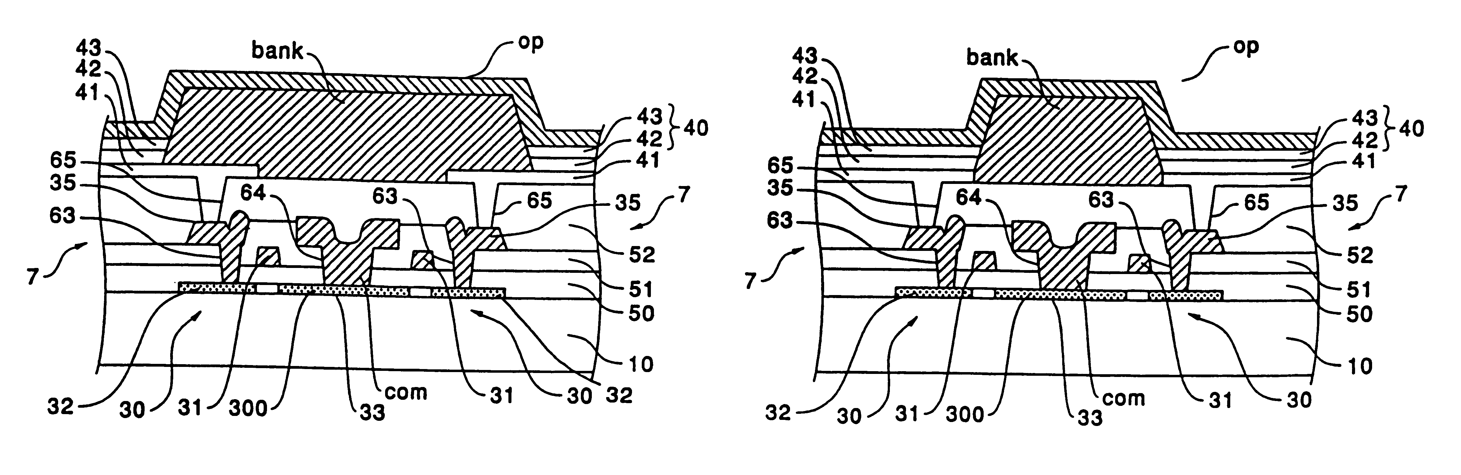
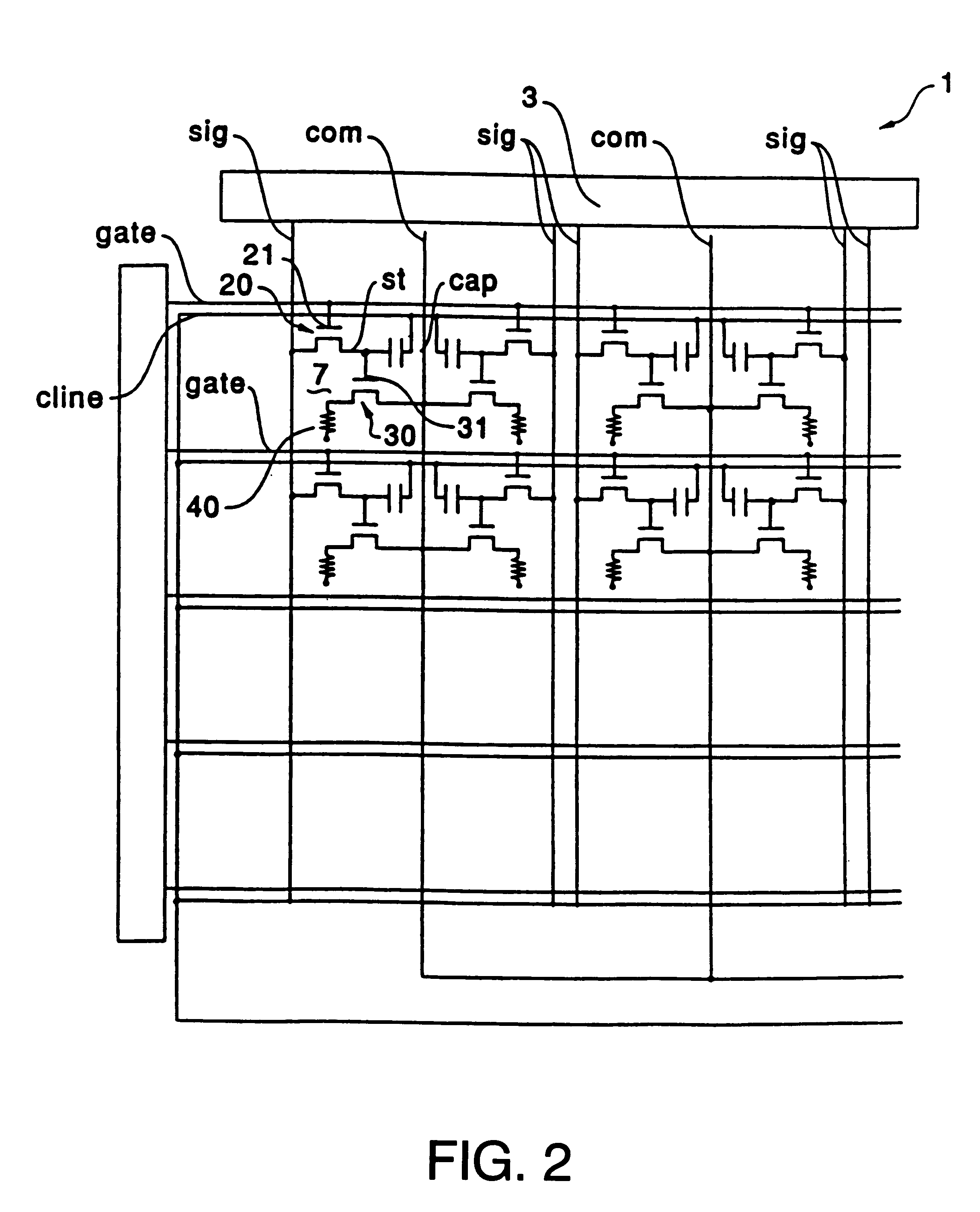
In the display device 1 according to the present embodiment, as shown in FIG. 1, a display area 2 is formed in the center of the surface of a transparent substrate 10 serving as a base member of the display device. In a peripheral area on the transparent substrate 10, a data line driving circuit 3 (first driving circuit) for outputting an image signal and a test circuit 5 are formed on respective sides at ends of data lines "sig", and scanning line driving circuits 4 (second driving circuits) for outputting a scanning signal are formed on respective sides at both ends of scanning lines ("gate"). In these driving circuits 3 and 4, a shift register, level shifters, and analog switches are formed using complementar...


PUM


Abstract

The invention provides a display device in which parasitic capacitance associated with data lines and driving circuits is prevented using a bank layer whose primary purpose is to define areas on a substrate in which an organic semiconductor film is formed. When the organic semiconductor film for forming a luminescent element such as an electroluminescent element or an LED is formed is formed in pixel regions (7), the organic semiconductor film is formed in the areas surrounded by the bank layer (bank) formed of a black resist. The bank layer (bank) is also formed between an opposite electrode (op) and data lines (sig) for supplying an image signal to first TFTs (20) and holding capacitors (cap) in the pixel regions (7) thereby preventing parasitic capacitance associated with the data lines (sig).

Description

1. Technical FieldThe present invention relates to an active matrix display device in which driving of luminescent elements such as LEDs (light emitting diodes) or EL (electroluminescent) elements which emit light when a driving current is passed through an organic semiconductor film is controlled by thin film transistors (hereinafter referred to as TFTs). More specifically, the present invention relates to a technique of optimizing the layout to improve the display performance.2. Description of Related ArtActive matrix display devices using current-controlled luminescent elements such as EL elements or LEDs have been proposed. Any types of luminescent elements used in display devices of this type have the capability of emitting light. Therefore, backlight is not required in display devices of this type unlike the liquid crystal display devices.FIG. 13 is a block diagram illustrating an example of such an active matrix display device in which carrier injection type organic thin film...

Claims


Application Information

Patent Timeline
IPC IPC(8): G09G3/32H01L27/28H01L27/32H01L51/52H01L51/50H05B33/26G09F9/30G09G3/00G09G3/20G09G3/30H01L27/00H05B33/12H05B33/14
CPCG09G3/3225H01L27/3246H01L27/3276G09G3/006G09G2300/0417G09G2300/0426G09G2300/0439G09G2300/0465G09G2300/0842G09G2300/0876G09G2320/0209H01L27/326H01L51/5284H01L2251/558H10K59/122H10K59/121H10K59/131H10K50/865H10K2102/351G09F9/30
Inventor OZAWA, TOKUROH
Owner INTELLECTUAL KEYSTONE TECH LLC
Why Eureka
Try Eureka