8 bit per cell non-volatile semiconductor memory structure utilizing trench technology and dielectric floating gate

a non-volatile semiconductor and memory structure technology, applied in semiconductor devices, electrical devices, instruments, etc., can solve the problems of poor reliability, difficult design and manufacture of multi-level storage cells,

Inactive Publication Date: 2001-03-20
MACRONIX INT CO LTD
View PDF10 Cites 320 Cited by
  • Summary
  • Abstract
  • Description
  • Claims
  • Application Information

AI Technical Summary

Problems solved by technology

As a result, multilevel storage cells are difficult to design and manufacture.
Some exhibit poor reliability.

Method used


Image

  • 8 bit per cell non-volatile semiconductor memory structure utilizing trench technology and dielectric floating gate
  • 8 bit per cell non-volatile semiconductor memory structure utilizing trench technology and dielectric floating gate
  • 8 bit per cell non-volatile semiconductor memory structure utilizing trench technology and dielectric floating gate

Examples


Embodiment Construction

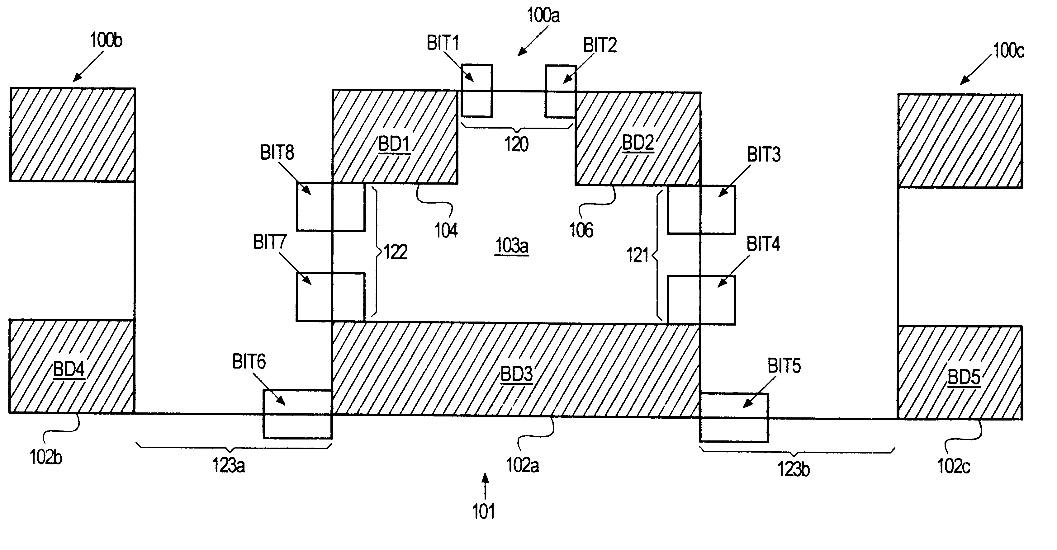
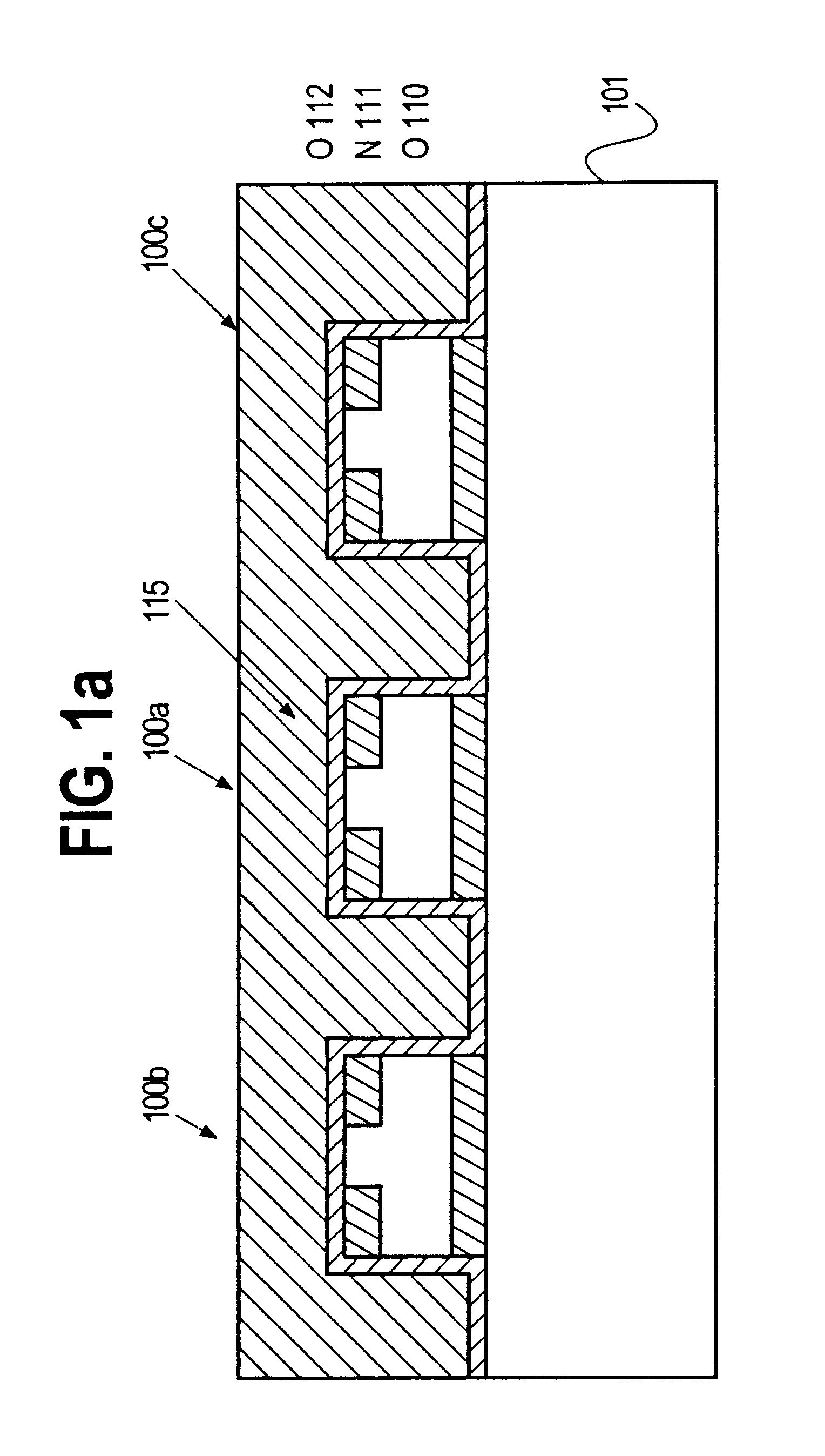
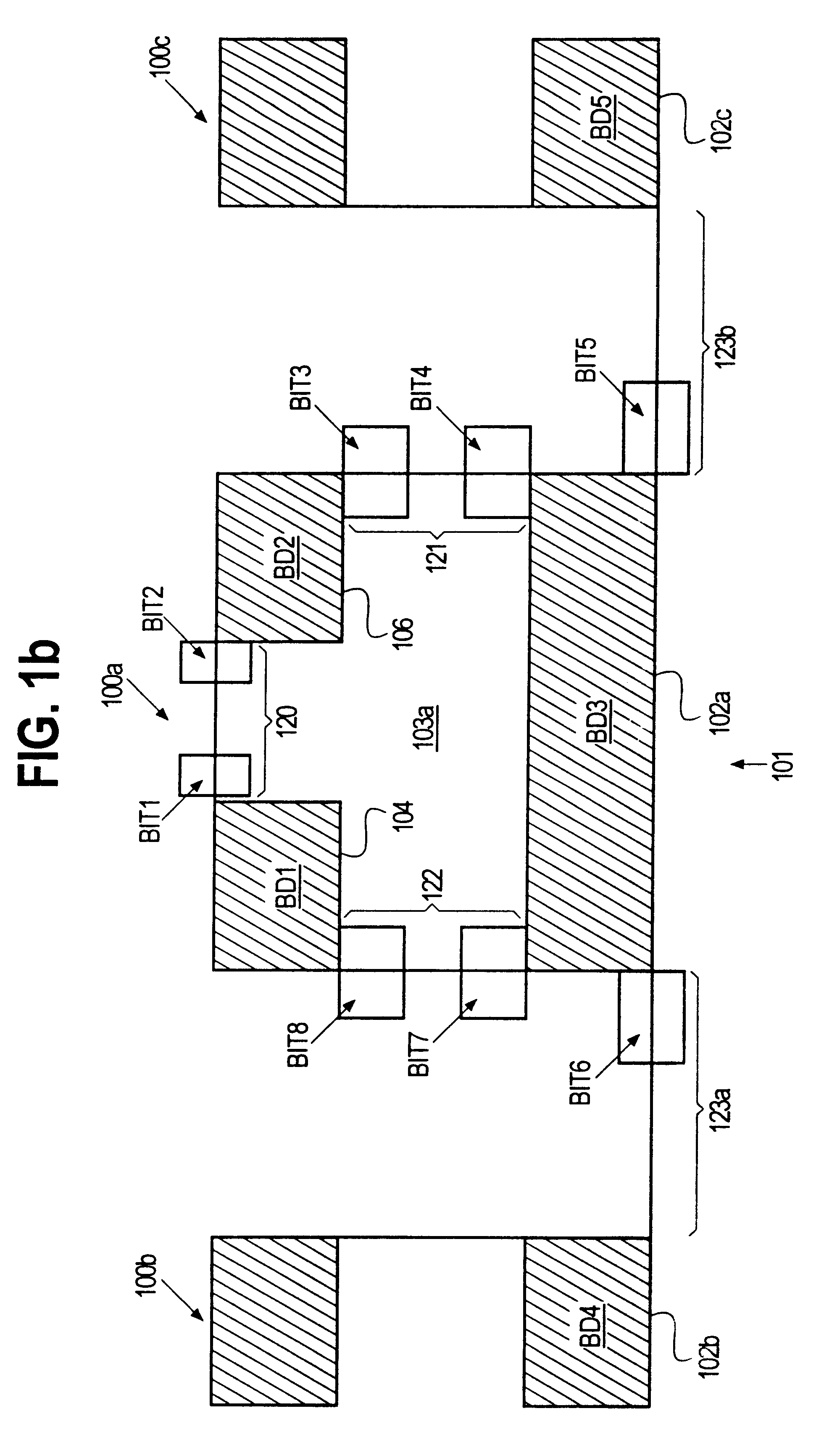
While the present invention may be embodied in many different forms and produced by various different fabrication processes, there is shown in the drawings and discussed herein one specific embodiment and fabrication method with the understanding that the present disclosure is to be considered only as an exemplification of the principles of the invention and is not intended to limit the invention to the embodiment illustrated.

FIGS. 1a and 1b show eight-bit non-volatile memory cell structures 100 that are formed on and incorporate a portion of semiconductor substrate 101 in association with the present invention. As each cell 100 is preferably constructed identically, the structure for cell 100a shall be described with the understanding that such structure is preferably found in each cell. Some memory cells varying from this main construct may be used in association with cell 100. In fact, it is contemplated that modified versions of cell 100 (and other types of cells) will likely be...


PUM


Abstract

The present application discloses a non-volatile semiconductor memory device for storing up to eight-bits of information. The device has a semiconductor substrate of one conductivity type, a central bottom diffusion region on top of a portion of the semiconductor substrate, a second semiconductor layer on top of the bottom diffusion region, and left and right diffusion regions formed in the second semiconductor layer apart from the central bottom diffusion region thus forming a first vertical channel between the right and central bottom diffusion regions. The device further includes a trapping dielectric layer formed over exposed portions of the semiconductor substrate, left, central and right bottom diffusion regions and second semiconductor layer and a wordline formed over the trapping dielectric layer. A methods of fabricating this novel cell using trench technology is also disclosed.

Description

1. Field of the InventionThe present invention relates in general to non-volatile digital memories and, more particularly, to an improved cell structure for a programmable non-volatile memory (such as conventional EEPROM or Flash EEPROM) that can store up to eight-bits of information and a method for fabricating same.2. Background ArtNon-volatile memory devices, such as EPROM, EEPROM, and flash EPROM devices, generally include a matrix of transistors which act as memory cells for storing a single-bit of information. Each transistor in this matrix has source and drain regions formed on a n- or p-type semiconductor substrate, a thin tunnel dielectric layer formed on the surface of the semiconductor substrate positioned at least between the source and drain regions, a floating gate (formed of polysilicon) positioned on the insulating layer for holding a charge, a control gate and an interpoly dielectric positioned between the floating gate and control gate.Traditionally, the interpoly ...

Claims


Application Information

Patent Timeline
Patent Type & Authority Patents(United States)
IPC IPC(8): H01L27/115H01L21/70H01L21/8246H01L29/66H01L29/792G11C16/02G11C16/04H01L21/8247H01L29/788
CPCH01L27/115H01L27/11568H01L29/7923H01L29/7926H10B43/30H10B69/00
Inventor LUNG, HSING LANLU, TAO CHENGWANG, MAM TSUNG
Owner MACRONIX INT CO LTD
Why Eureka
Try Eureka