Method of producing a multi-layer ceramic substrate

Inactive Publication Date: 2001-05-08
MURATA MFG CO LTD
View PDF22 Cites 55 Cited by
  • Summary
  • Abstract
  • Description
  • Claims
  • Application Information

AI Technical Summary

Problems solved by technology

However, the method has the following problems:
(1) Due to comparatively large irregularity in the paste film thickness and printing displacement, the irregularity in the capacitor characteristics such as the capacity is comparatively large.
(2) Paste deformation generated in the pressing or baking step gives rise to the irregularity in the characteristics such as the capacity.
(3) Due to deterioration of the flatness in the printing part according to the repetition of printing and lamination, it is difficult to increase the number of the lamination so that a large capacity can hardly be achieved in a capacitor.
However, this method has the following problems substantially the same as those of the above-mentioned first method:
(1) Characteristics irregularity due to the printing pattern displacement and the film thickness irregularity,
(2) Capacity limitation due to the difficulty in increasing the number of the lamination, and
Accordingly, although problems including the characteristics irregularity such as capacity and limitation with respect to a larger capacity can be solved, the following problems come out:
(1) Since a laminated member containing plural kinds of sheets with different compositions is co-sintered, a highly sophisticated technology is required in controlling the contraction behavior and the heat expansion coefficient so as to be coincided in t

Method used


Image

  • Method of producing a multi-layer ceramic substrate
  • Method of producing a multi-layer ceramic substrate
  • Method of producing a multi-layer ceramic substrate

Examples


Embodiment Construction

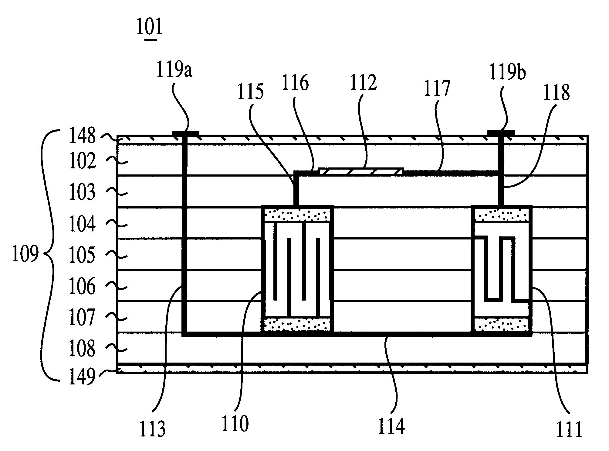
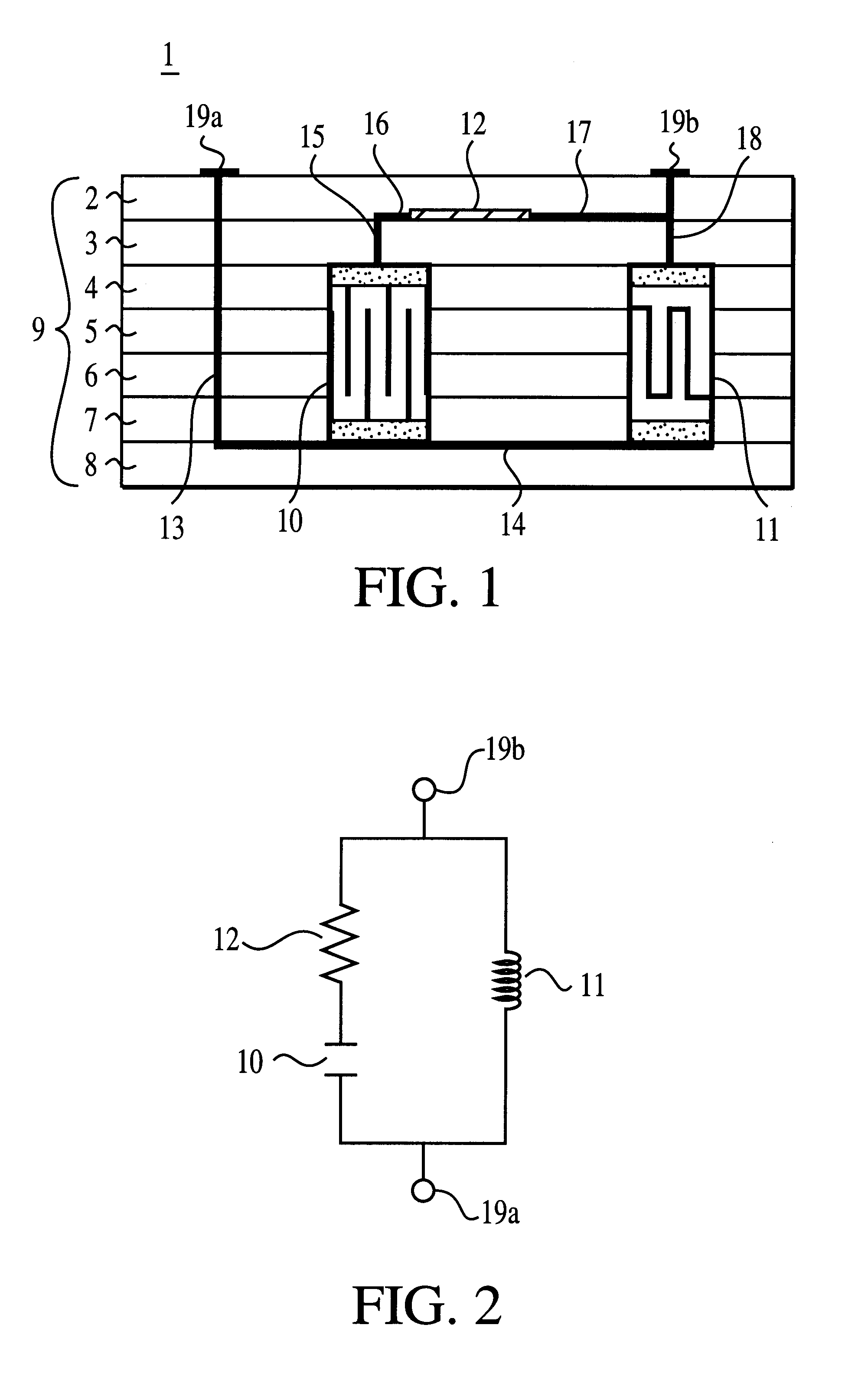
FIG. 1 is a cross-sectional view schematically showing a multi-layer ceramic substrate 1 according to a first preferred embodiment of the present invention. FIG. 2 is an equivalent circuit diagram provided by the multi-layer substrate 1 shown in FIG. 1.

As shown in FIG. 1, the multi-layer ceramic substrate 1 comprises a laminated member 9 having a plurality of laminated ceramic layers made of a ceramic insulating material 2, 3, 4, 5, 6, 7 and 8. The laminated member 9 accommodates a capacitor 10, an inductor 11 and a resistor 12 as the passive components. Furthermore, the laminated member 9 accommodates wiring conductors 13, 14, 15, 16, 17 and 18 for wiring the capacitor 10, the inductor 11, and the resistor 12, and further, has external terminal conductors 19a and 19b on the outer surface. Accordingly, the multi-layer ceramic substrate 1 provides a circuit as shown in FIG. 2.

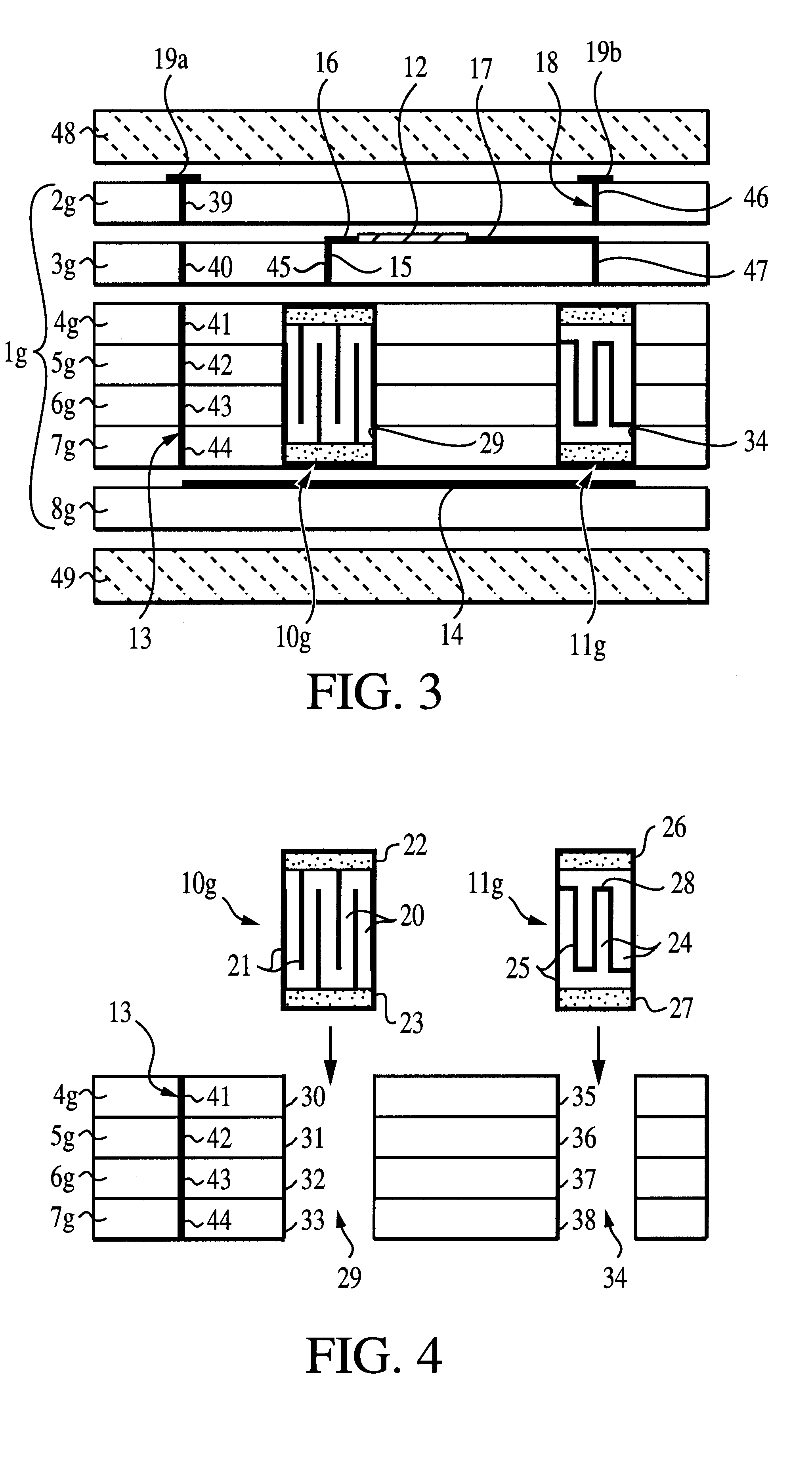
The multi-layer ceramic substrate 1 with the above-mentioned configuration can be produced as follows. FIG. 3...


PUM

PropertyMeasurementUnit
Timeaaaaaaaaaa
Linear densityaaaaaaaaaa
Angleaaaaaaaaaa

Abstract

The invention provides a method of producing a multi-layer ceramic substrate comprising a laminated member having a plurality of ceramic layers made of a ceramic insulating material and a wiring conductor, comprising the steps of: preparing a raw compact having the plurality of the laminated ceramic green sheets containing the ceramic insulating material and the wiring conductor; providing raw sheet type bases on the principal plane at both ends with respect to the lamination direction of the raw compact, the raw sheet type bases containing a ceramic not to be sintered at the baking temperature of the raw compact; baking the raw compact in the state interposed between the sheet type bases so as to obtain the laminated member; and eliminating the unsintered sheet type bases; wherein the heat expansion coefficient difference of the sheet type bases and the laminated member after baking is 2.5x10⁻⁶ degK-1 or more.

Description

1. Field of the InventionThe present invention relates to a method of producing a multi-layer ceramic substrate. Specifically, it relates to a method of producing a multi-layer ceramic substrate to be adopted advantageously in the production of a multi-layer ceramic substrate accommodating a passive component such as a capacitor, an inductor, or the like.2. Description of the Related ArtIn order to realize multi-functions, a higher density, and a higher performance in a multi-layer circuit substrate represented by a multi-layer ceramic substrate, it is effective to store a sophisticated passive component and apply wiring with a high density in such a multi-layer circuit substrate.Multi-layer circuit substrates storing a passive component accordingly have been produced conventionally by various methods as follows:First one is a so-called thick film method where a dielectric paste, or the like, is printed on substrate green sheets by the thick film forming technology so that the green...

Claims


Application Information

Patent Timeline
IPC IPC(8): H01L21/48H01L21/02H05K1/16H01L23/12
CPCH01L21/4857H05K1/16H05K1/186H05K1/0306H05K3/4629H05K2201/10636Y02P70/50H01L23/12
Inventor SAKAMOTO, SADAAKISUNAHARA, HIROFUMINISHIDE, MITSUYOSHI
Owner MURATA MFG CO LTD
Why Eureka
Try Eureka